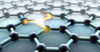
At Washington University in St. Louis, a group of physicists found a way to locally add a charge to an atomically thin graphene device by adding another thin sheet of a thin material called α-RuCl3 to a multilayer thin sheet.
In a study published in the journal Nano Letters, the researchers provided a detailed description of the charge transfer process. It is essential that the current flowing through the atomically thin materials must be controlled to ensure future potential applications in computing or photovoltaics.
In my field, we study van der Waals force heterostructures formed by custom stacking atomically thin materials. We usually control the charge by applying an electric field to the device. But it now appears that we can only add the RuCl3 layer. It absorbs a fixed amount of electrons, allowing us to perform a "permanent" charge transfer that does not require an external electric field. Said Erik Henriksen, assistant professor of physics at Washington University School of Arts and Sciences in St. Louis.
Physics professor Li Yang and his graduate student Lu Xiaobo performed calculations and calculations separately. They are both co-authors of the University of Washington's research.
Physicists studying condensed matter have focused their attention on α-RuCl3 because they want to use its antiferromagnetic properties to realize quantum spin liquids. In this new study, the research team reported that α-RuCl3 can transfer charge to many different types of materials, not only graphene but Henriksen's personal favorite.
The researchers also found that just placing a layer of α-RuCl3 on top of their device is sufficient to generate and transfer charge. Even if a thin sheet of electrically insulating material slides between graphene and RuCl3, the process is still effective.
We can control how much charge flows in by changing the thickness of the insulator. Moreover, we can physically and spatially separate the charge source from the charge source, which is called modulation doping. Whenever you do this, it becomes exciting. Usually, you have to add atoms to bulk materials, which can cause a lot of confusion. But here, the charge flows indirectly, without changing the chemical structure, so this is a "clean" way of extra charge.