


1. Características básicas ne variedad cristalografía carburo silicio
1.1 Estructura atómica ne complejidad politípica
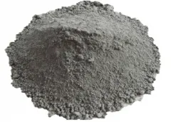
(Polvo carburo silicio)
Carburo silicio (SiC) is a binary substance made up of silicon and carbon atoms set up in an extremely steady covalent latticework, identified by its extraordinary hardness, conductividad térmica,, and digital residential properties.
Unlike conventional semiconductors such as silicon or germanium, SiC does not exist in a single crystal structure however manifests in over 250 distinctive polytypes– crystalline types that differ in the piling sequence of silicon-carbon bilayers along the c-axis.
The most highly relevant polytypes consist of 3C-SiC (cubic, zincblende framework), 4H-SiC, and 6H-SiC (both hexagonal), each showing subtly various digital and thermal attributes.
Among these, 4H-SiC is especially preferred for high-power and high-frequency digital gadgets as a result of its higher electron flexibility and lower on-resistance contrasted to various other polytypes.
Ar xí nze̲di enlace covalente– comprende ar hmädi 88% covalente ne 12% ya nt'ot'e iónico– proporciona notable dureza mecánica, inercia química, ne resistencia ja ya daños radiación, o̲t'e SiC mfädi pa ar procesamiento jar entornos extremos.
1.2 Propiedades electrónicas ne térmicas
Ar superioridad electrónica ar SiC surge ár nt'ot'e ho 'bui ndunthe bandgap, da varía ar 2.3 eV (3C — SiC) to 3.3 eV (4H-SiC), xingu mäs dätä nä'ä ar silicio 1.1 eV.
nuna Nar dätä hño bandgap permite da dispositivos SiC operan temperaturas xingu mäs altas– tanto komo 600 ° C– hinda generación portadora intrínseca abrumando ar dispositivo, 'nar ja crucial jar dispositivos electrónicos basados jar silicio.
Furthermore, SiC pe̲ts'i 'nar mextha resistencia hwähi eléctrico crítico (~ 3 MV yá cm), 'ra 're̲t'a ya 'nandi nä'ä ar silicio, permitiendo mäs delgadas capas deriva ne voltajes ar avería mäs altos jar dispositivos nts'edi.
ár conductividad térmica (~ 3.7– 4.9 W yá cm · Kë pa 4 H — SiC) supera ar cobre, ayudando jar disipación pa nt'ot'e xi hño ne reducir ar 'medi da sistemas enfriamiento complejos jar aplicaciones mextha nts'edi.
incorporado ko mextha velocidad saturación electrones (~ 2 × 10 10^7 cm yá s), gi estructuras permiten transistores ne diodos basados jar SiC mpa̲ti mäs ngutha, manejar voltajes mäs altos, ne operar ko mäs xi hño dätä nt'ot'e energética da homólogos silicio.
gi propiedades colectivamente o̲t'e ar SiC 'nar he̲'mi clave pa ar electrónica nts'edi Nu'bu̲ ar generación, particularmente jar vehículos eléctricos, sistemas energía renovables, ne tecnologías aeroespaciales.
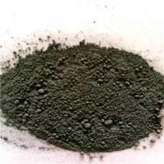
( Polvo carburo silicio)
2. síntesis ne fabricación cristales carburo silicio mextha ar hño
2.1 crecimiento ya xito granel a través de transporte físico vapores
producción mextha pureza, SiC monocristal ge 'na ya 'na'ño instituto mäs desafiantes ár nt'ot'e técnica, mostly because of its high sublimation temperature (~ 2700 ° C )and complex polytype control.
The leading technique for bulk growth is the physical vapor transportation (PVT) strategy, additionally referred to as the modified Lely method, in which high-purity SiC powder is sublimated in an argon atmosphere at temperatures surpassing 2200 ° C and re-deposited onto a seed crystal.
Exact control over temperature slopes, gas circulation, and pressure is important to lessen defects such as micropipes, dislocations, and polytype additions that degrade device efficiency.
Despite advances, the growth rate of SiC crystals continues to be slow– usually 0.1 to 0.3 mm/h– making the process energy-intensive and pricey compared to silicon ingot manufacturing.
Continuous research focuses on enhancing seed orientation, doping harmony, and crucible layout to enhance crystal top quality and scalability.
2.2 Epitaxial Layer Deposition and Device-Ready Substratums
For digital device fabrication, a slim epitaxial layer of SiC is expanded on the bulk substratum using chemical vapor deposition (CVD), usually using silane (SiH ₄) and lp (C ₃ H EIGHT) as forerunners in a hydrogen ambience.
This epitaxial layer must show accurate density control, reduced defect density, and tailored doping (with nitrogen for n-type or light weight aluminum for p-type) to create the energetic regions of power gadgets such as MOSFETs and Schottky diodes.
The latticework inequality in between the substratum and epitaxial layer, together with recurring stress from thermal growth differences, can present piling faults and screw dislocations that affect tool reliability.
Advanced in-situ surveillance and process optimization have actually substantially decreased flaw densities, making it possible for the business production of high-performance SiC gadgets with lengthy operational lifetimes.
adicionalmente, the advancement of silicon-compatible processing methods– such as completely dry etching, ion implantation, and high-temperature oxidation– has helped with combination into existing semiconductor manufacturing lines.
3. Applications in Power Electronic Devices and Energy Solution
3.1 High-Efficiency Power Conversion and Electric Mobility
Silicon carbide has actually come to be a keystone material in modern power electronic devices, where its ability to switch over at high frequencies with very little losses translates right into smaller sized, mäs ligero, and extra reliable systems.
In electrical cars (EVs), SiC-based inverters transform DC battery power to air conditioning for the electric motor, running at frequencies as much as 100 kHz– dramatically more than silicon-based inverters– decreasing the size of passive parts like inductors and capacitors.
This results in enhanced power thickness, extended driving variety, and enhanced thermal management, directly attending to vital obstacles in EV style.
Significant automotive manufacturers and providers have taken on SiC MOSFETs in their drivetrain systems, achieving power financial savings of 5– 10% contrasted to silicon-based options.
Xkagentho modo, in onboard chargers and DC-DC converters, SiC gadgets allow much faster charging and higher performance, accelerating the transition to lasting transportation.
3.2 Renewable Resource and Grid Framework
In photovoltaic (PV) solar inverters, SiC power components boost conversion performance by reducing switching and conduction losses, especially under partial tons problems common in solar power generation.
This enhancement raises the general energy return of solar setups and lowers cooling requirements, reducing system prices and enhancing reliability.
In wind generators, SiC-based converters deal with the variable frequency outcome from generators a lot more effectively, allowing better grid combination and power high quality.
Past generation, SiC is being deployed in high-voltage direct existing (HVDC) transmission systems and solid-state transformers, where its high malfunction voltage and thermal security support compact, high-capacity power distribution with minimal losses over fars away.
Nuya avances ya esenciales pa mejorar ya redes eléctricas envejecimiento ne acomodar ar creciente cuota dispersos ne intermitentes recursos respetuosos ar nt'uni mbo jar ximha̲i.
4. Roles emergentes jar extremo ar nt'uni mbo jar ximha̲i ne tecnologías cuánticas
4.1 Operación jar hñäki extremos: Aerospace, Nuclear, ne aplicaciones pozo profundo
Robustez ar SiC extiende ar electrónica ja ya entornos ho fallan ya productos estándar.
Ja ya sistemas aeroespaciales ne mfats'i, Sensores SiC ne dispositivos electrónicos funcionan con precisión mextha ar mpat'i, nkohi mextha ar radiación cerca de motores a reacción, vehículos re-entrada, ne sondas espaciales.
Ár dureza radiación bí thogi ar ideal pa monitoreo central nuclear ne electrónica satélite, ho exposición radiación ionizante tsa̲ da degradar ya dispositivos silicio.
Ja ar sector petróleo ne gas, SiC-based sensing units are utilized in downhole drilling devices to withstand temperature levels going beyond 300 ° C and corrosive chemical environments, allowing real-time data purchase for improved removal performance.
These applications leverage SiC’s ability to preserve architectural honesty and electric functionality under mechanical, Térmico, and chemical stress and anxiety.
4.2 Combination right into Photonics and Quantum Sensing Operatings Systems
Past classical electronic devices, SiC is emerging as an encouraging system for quantum technologies because of the visibility of optically active factor flaws– such as divacancies and silicon vacancies– that display spin-dependent photoluminescence.
These defects can be adjusted at room temperature level, acting as quantum bits (qubits) or single-photon emitters for quantum interaction and picking up.
The broad bandgap and low inherent service provider focus enable long spin coherence times, essential for quantum data processing.
Furthermore, SiC is compatible with microfabrication strategies, allowing the integration of quantum emitters into photonic circuits and resonators.
This mix of quantum capability and commercial scalability placements SiC as a special product bridging the space in between fundamental quantum science and useful device engineering.
In summary, silicon carbide stands for a standard change in semiconductor modern technology, using unequaled performance in power effectiveness, thermal management, and ecological durability.
From making it possible for greener energy systems to sustaining exploration in space and quantum worlds, SiC remains to redefine the limits of what is highly feasible.
Vendor
RBOSCHCO ge 'nar proveedor he̲'mi químico global confiable & Fabricante ko nä'ä 12 ya je̲ya mfeni jar proveer productos químicos ne nanomateriales súper mextha ar hño. Ar empresa exporta xingu ya ximha̲i, komongu ar EE.UU., Canadá, Europa, Emiratos ar Árabe Unidos, Sudáfrica, Tanzania, Kenia, Egipto, Nigeria, Camerún, Uganda, Turquía, M'onda, Azerbaiyán, Bélgica, Chipre, Czech Republic, Brazil, Chile, Argentina, Dubai, Japan, Korea, Vietnam, Thailand, Malaysia, Indonesia, Australia,Germany, France, Italy, Portugal etc. As a leading nanotechnology development manufacturer, RBOSCHCO dominates the market. Our professional work team provides perfect solutions to help improve the efficiency of various industries, create value, and easily cope with various challenges. If you are looking for sic compound, Jaki pe̲hni 'nar correo ma: [email protected]
Tags: carburo silicio,mosfet carburo silicio,mosfet sic
All articles and pictures are from the Internet. If there are any copyright issues, please contact us in time to delete.
Inquiry us