


1. Кристалічний каркас і розділена анізотропія
1.1 Поліморфи 2H і 1T: Архітектурна та цифрова подвійність
(Дисульфід молібдену)
Дисульфід молібдену (MoS TWO) is a split transition steel dichalcogenide (TMD) with a chemical formula including one molybdenum atom sandwiched in between two sulfur atoms in a trigonal prismatic coordination, утворюючи ковалентний зв’язок S– пн– S аркушів.
These specific monolayers are piled vertically and held with each other by weak van der Waals forces, allowing very easy interlayer shear and exfoliation down to atomically thin two-dimensional (2Д) кристали– an architectural function main to its varied useful duties.
MoS ₂ exists in multiple polymorphic kinds, the most thermodynamically steady being the semiconducting 2H stage (hexagonal symmetry), де кожен шар показує пряму ширину забороненої зони ~ 1.8 еВ у моношаровому типі, який переходить до непрямої забороненої зони (~ 1.3 еВ) wholesale, a phenomenon vital for optoelectronic applications.
З іншого боку, метастабільна фаза 1Т (tetragonal balance) takes on an octahedral coordination and acts as a metallic conductor because of electron contribution from the sulfur atoms, making it possible for applications in electrocatalysis and conductive compounds.
Stage transitions in between 2H and 1T can be induced chemically, електрохімічно, or via pressure design, supplying a tunable platform for designing multifunctional devices.
The capacity to support and pattern these phases spatially within a solitary flake opens paths for in-plane heterostructures with unique electronic domains.
1.2 дефекти, Допінг, і побічні держави
The performance of MoS two in catalytic and digital applications is highly conscious atomic-scale issues and dopants.
Innate point problems such as sulfur openings act as electron contributors, raising n-type conductivity and working as active websites for hydrogen advancement reactions (ЇЇ) у розщепленні води.
Grain borders and line problems can either restrain fee transport or produce local conductive paths, relying on their atomic configuration.
Regulated doping with change metals (напр., Re, Nb) або халькогени (напр., Se) allows fine-tuning of the band framework, provider concentration, and spin-orbit combining results.
Значно, the sides of MoS two nanosheets, particularly the metal Mo-terminated (10– 10) edges, display significantly greater catalytic activity than the inert basal airplane, inspiring the layout of nanostructured stimulants with made best use of edge exposure.
( Дисульфід молібдену)
These defect-engineered systems exemplify how atomic-level manipulation can change a normally happening mineral into a high-performance practical material.
2. Стратегії синтезу та нанофабрикації
2.1 Bulk and Thin-Film Manufacturing Approaches
Природний молібденіт, the mineral form of MoS ₂, has actually been used for years as a strong lube, but modern-day applications require high-purity, structurally controlled artificial kinds.
Хімічне осадження з парової фази (ССЗ) is the leading technique for generating large-area, high-crystallinity monolayer and few-layer MoS ₂ films on substrates such as SiO TWO/ Si, сапфір, or adaptable polymers.
При ССЗ, прекурсори молібдену та сірки (напр., MoO чотири і порошок S) are vaporized at heats (700– 1000 ° C )under controlled environments, allowing layer-by-layer development with tunable domain dimension and alignment.
Mechanical exfoliation (“підхід скотчем”) continues to be a standard for research-grade samples, створюючи надчисті моношари з невеликими дефектами, хоча він не має масштабованості.
Рідкофазний пілінг, including sonication or shear blending of mass crystals in solvents or surfactant solutions, generates colloidal dispersions of few-layer nanosheets suitable for finishings, composites, і склади чорнила.
2.2 Heterostructure Combination and Device Pattern
Truth potential of MoS ₂ emerges when incorporated right into vertical or lateral heterostructures with various other 2D materials such as graphene, гексагональний нітрид бору (h-BN), or WSe ₂.
These van der Waals heterostructures enable the layout of atomically exact devices, including tunneling transistors, фотодетектори, і світлодіоди (світлодіоди), where interlayer fee and power transfer can be crafted.
Lithographic patterning and etching strategies enable the fabrication of nanoribbons, квантові точки, і польові транзистори (польові транзистори) with channel sizes to tens of nanometers.
Dielectric encapsulation with h-BN secures MoS ₂ from environmental destruction and decreases fee spreading, significantly boosting service provider flexibility and tool security.
These construction advances are vital for transitioning MoS two from lab curiosity to feasible component in next-generation nanoelectronics.
3. Functional Features and Physical Mechanisms
3.1 Tribological Habits and Strong Lubrication
Among the oldest and most enduring applications of MoS ₂ is as a dry strong lube in extreme environments where liquid oils fall short– наприклад, пилосос, heats, or cryogenic conditions.
The reduced interlayer shear strength of the van der Waals void permits very easy sliding in between S– пн– S шарів, в результаті чого коефіцієнт тертя зменшується до 0,03– 0.06 under ideal problems.
Its performance is further enhanced by strong adhesion to metal surface areas and resistance to oxidation as much as ~ 350 °C на повітрі, beyond which MoO five formation boosts wear.
MoS ₂ is widely used in aerospace systems, air pump, and gun components, typically used as a finish by means of burnishing, розпилення, або об'єднання композитів у полімерні матриці.
Recent studies show that humidity can weaken lubricity by raising interlayer bond, prompting research right into hydrophobic coatings or hybrid lubes for better environmental stability.
3.2 Electronic and Optoelectronic Feedback
As a direct-gap semiconductor in monolayer kind, MoS ₂ exhibits solid light-matter interaction, з перевищенням коефіцієнтів поглинання 10 ⁵ centimeters ⁻¹ and high quantum return in photoluminescence.
This makes it ideal for ultrathin photodetectors with quick action times and broadband level of sensitivity, від видимого до ближнього інфрачервоного діапазону.
Field-effect transistors based on monolayer MoS ₂ demonstrate on/off ratios > 10 eight and provider wheelchairs up to 500 centimeters ²/ V · s in suspended examples, though substrate interactions usually restrict practical worths to 1– 20 см ДВА/ V · с.
Спін-долинне комбінування, an effect of strong spin-orbit interaction and busted inversion balance, enables valleytronics– a novel paradigm for information inscribing utilizing the valley level of flexibility in momentum space.
These quantum phenomena setting MoS ₂ as a candidate for low-power logic, пам'ять, and quantum computer aspects.
4. Програми в Power, каталіз, та новітні технології
4.1 Electrocatalysis for Hydrogen Evolution Response (ЇЇ)
MoS two has become an appealing non-precious choice to platinum in the hydrogen evolution reaction (ЇЇ), an essential procedure in water electrolysis for green hydrogen production.
While the basal airplane is catalytically inert, edge sites and sulfur jobs display near-optimal hydrogen adsorption complimentary power (ΔG_H * ≈ 0), similar to Pt.
Nanostructuring techniques– such as developing up and down straightened nanosheets, defect-rich movies, or drugged hybrids with Ni or Co– maximize active website thickness and electric conductivity.
When integrated into electrodes with conductive sustains like carbon nanotubes or graphene, MoS two accomplishes high existing densities and long-lasting stability under acidic or neutral conditions.
Additional enhancement is attained by stabilizing the metal 1T stage, which boosts intrinsic conductivity and reveals added energetic websites.
4.2 Versatile Electronic Devices, Датчики, і квантові пристрої
The mechanical flexibility, transparency, and high surface-to-volume proportion of MoS two make it excellent for flexible and wearable electronic devices.
Транзистори, логічні схеми, and memory tools have actually been shown on plastic substratums, allowing bendable display screens, відображення здоров'я, and IoT sensing units.
MoS TWO-based gas sensing units display high level of sensitivity to NO TWO, NH ДВА, and H TWO O as a result of bill transfer upon molecular adsorption, with response times in the sub-second array.
У квантових сучасних технологіях, MoS two hosts localized excitons and trions at cryogenic temperature levels, and strain-induced pseudomagnetic fields can trap carriers, enabling single-photon emitters and quantum dots.
These growths highlight MoS two not only as a functional product however as a system for checking out essential physics in minimized measurements.
Підсумовуючи, molybdenum disulfide exemplifies the merging of timeless products science and quantum engineering.
From its ancient role as a lubricating substance to its modern-day release in atomically thin electronic devices and power systems, MoS ₂ remains to redefine the borders of what is possible in nanoscale products style.
Як синтез, характеристика, and assimilation techniques advancement, its effect across science and innovation is poised to expand also better.
5. Провайдер
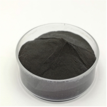
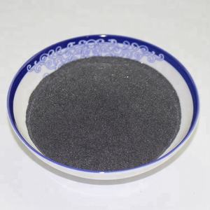
TRUNNANO є всесвітньо визнаним виробником і постачальником дисульфіду молібдену з більш ніж 12 років досвіду у найякісніших наноматеріалах та інших хімікатах. Компанія розробляє різноманітні порошкові матеріали та хімічні речовини. Надання послуг OEM. Якщо вам потрібен високоякісний дисульфід молібдену, будь ласка, не соромтеся зв'язатися з нами. Ви можете натиснути на товар, щоб зв’язатися з нами.
Теги: Дисульфід молібдену, нано дисульфід молібдену, MoS2
Всі статті та фотографії взяті з Інтернету. Якщо є проблеми з авторським правом, будь ласка, зв'яжіться з нами вчасно, щоб видалити.
Зверніться до нас