


1. Crystal Framework ati Pipin Anisotropy
1.1 Awọn 2H ati 1T Polymorphs: Ayaworan ati Digital Duality
(Molybdenum Disulfide)
Molybdenum disulfide (MOS MEJI) jẹ pipin iyipada irin dichalcogenide (TMD) pẹlu agbekalẹ kemikali kan pẹlu ọkan molybdenum atom sandwiched laarin awọn ọta imi imi-ọjọ meji ni isọdọkan prismatic trigonal kan, ti n dagba ni iṣọkan S– Mo– S awọn iwe.
Awọn monolayers pato wọnyi ni a kojọpọ ni inaro ati waye pẹlu ara wọn nipasẹ awọn ologun van der Waals alailagbara, gbigba rirẹ-irun interlayer rọrun pupọ ati exfoliation si isalẹ lati atomically tinrin onisẹpo meji (2D) kirisita– iṣẹ ayaworan ni akọkọ si awọn iṣẹ iwulo oriṣiriṣi rẹ.
MoS ₂ wa ni ọpọlọpọ awọn oriṣi polymorphic, Iduro thermodynamic julọ julọ ni ipele 2H semiconducting (onígun mẹ́fà), ibi ti kọọkan Layer fihan kan ni gígùn bandgap ti ~ 1.8 eV ni oriṣi monolayer ti o yipada si bandgap aiṣe-taara (~ 1.3 eV) osunwon, lasan pataki fun awọn ohun elo optoelectronic.
Ti a ba tun wo lo, awọn metastable 1T alakoso (iwọntunwọnsi tetragonal) gba isọdọkan octahedral kan o si ṣe bii adaorin irin nitori idasi elekitironi lati awọn ọta imi-ọjọ imi-ọjọ., ṣiṣe awọn ti o ṣee ṣe fun awọn ohun elo ni electrocatalysis ati conductive agbo.
Awọn iyipada ipele laarin 2H ati 1T le ṣe ifilọlẹ ni kemikali, electrochemically, tabi nipasẹ apẹrẹ titẹ, n pese ipilẹ ti o le ṣatunṣe fun apẹrẹ awọn ẹrọ multifunctional.
Agbara lati ṣe atilẹyin ati apẹrẹ awọn ipele wọnyi ni aye laarin flake solitary ṣi awọn ipa ọna fun awọn ile-iṣẹ heterostructures inu ọkọ ofurufu pẹlu awọn ibugbe itanna alailẹgbẹ.
1.2 Awọn abawọn, Doping, ati Apa States
Iṣiṣẹ ti MoS meji ni katalitiki ati awọn ohun elo oni-nọmba jẹ awọn ọran iwọn atomiki mimọ gaan ati awọn dopants.
Awọn iṣoro aaye innate gẹgẹbi awọn ṣiṣi imi-ọjọ ṣe bi awọn oluranlọwọ elekitironi, igbega n-type conductivity ati ṣiṣẹ bi awọn oju opo wẹẹbu ti nṣiṣe lọwọ fun awọn aati ilosiwaju hydrogen (RẸ) ni omi pipin.
Awọn aala ọkà ati awọn iṣoro laini le ṣe idaduro gbigbe gbigbe ọya tabi gbejade awọn ipa ọna adaṣe agbegbe, gbigbe ara lori wọn atomiki iṣeto ni.
Doping ti a ṣe ilana pẹlu awọn irin iyipada (f.eks., Tun, Nb) tabi chacogens (f.eks., Se) faye gba itanran-yiyi ti awọn ilana iye, ifọkansi olupese, ati omo ere-orbit apapọ awọn esi.
Ni pataki, awọn ẹgbẹ ti MoS meji nanosheets, paapa irin Mo-opin (10– 10) egbegbe, ṣe afihan iṣẹ ṣiṣe katalitiki ti o tobi pupọ ju ọkọ ofurufu basali inert lọ, imoriya awọn ifilelẹ ti awọn nanostructured stimulants pẹlu ti o dara ju lilo ti ifihan eti.
( Molybdenum Disulfide)
Awọn ọna ṣiṣe-aṣiṣe-aṣiṣe wọnyi ṣe apẹẹrẹ bii ifọwọyi-ipele atomiki le yi ohun alumọni ti n ṣẹlẹ deede pada si ohun elo to wulo ti o ga julọ..
2. Iṣagbepọ ati Awọn ilana Nanofabrication
2.1 Olopobobo ati Tinrin-Fiimu Awọn ọna iṣelọpọ
Molybdenite adayeba, fọọmu nkan ti o wa ni erupe ile ti MoS ₂, ti kosi a ti lo fun odun bi kan to lagbara lube, ṣugbọn awọn ohun elo ode oni nilo mimọ-giga, Awọn iru atọwọda ti a ṣakoso ni igbekale.
Iṣagbejade oru kemikali (CVD) ni awọn asiwaju ilana fun ti o npese tobi-agbegbe, monolayer giga-crystallinity ati awọn fiimu MoS ₂ Layer diẹ lori awọn sobusitireti bii SiO TWO/ Si, oniyebiye, tabi awọn polima adaptable.
Ninu CVD, molybdenum ati imi-ọjọ ṣaaju (f.eks., MoO mẹrin ati S lulú) ti wa ni vaporized ni awọn ooru (700– 1000 ° C )labẹ iṣakoso awọn agbegbe, ngbanilaaye idagbasoke Layer-nipasẹ-Layer pẹlu iwọn-ašẹ tunable ati titete.
Exfoliation darí (“scotch teepu ona”) tẹsiwaju lati jẹ boṣewa fun awọn ayẹwo-ite iwadi, ti o npese olekenka-mimọ monolayers pẹlu ala awọn abawọn, bi o tilẹ jẹ pe ko ni scalability.
Liquid-ipele peeling, pẹlu sonication tabi irẹrun parapo ti ibi-krisita ni olomi tabi surfactant solusan, n ṣe awọn pipinka colloidal ti awọn nanosheets Layer diẹ ti o dara fun awọn ipari, awọn akojọpọ, ati inki formulations.
2.2 Apapọ Heterostructure ati Apẹẹrẹ Ẹrọ
Agbara otitọ ti MoS ₂ farahan nigba ti a dapọ taara si inaro tabi awọn ẹya heterostructures ita pẹlu ọpọlọpọ awọn ohun elo 2D miiran bii graphene, boron nitride hexagonal (h-BN), tabi WSe ₂.
Awọn wọnyi ni van der Waals heterostructures jeki awọn ifilelẹ ti awọn atomically gangan awọn ẹrọ, pẹlu tunneling transistors, fotodetectors, ati ina-emitting diodes (Awọn LED), nibiti owo interlayer ati gbigbe agbara le ṣe.
Ilana lithographic ati awọn ilana etching jẹ ki iṣelọpọ awọn nanoribbons ṣiṣẹ, kuatomu aami, ati awọn transistors ipa aaye (Awọn FET) pẹlu awọn iwọn ikanni si mewa ti nanometers.
Dielectric encapsulation pẹlu h-BN ṣe aabo MoS ₂ lati iparun ayika ati dinku itankale owo, significantly igbelaruge olupese iṣẹ ni irọrun ati aabo ọpa.
Awọn ilọsiwaju ikole wọnyi jẹ pataki fun iyipada MoS meji lati iwariiri lab si paati ti o ṣeeṣe ni awọn nanoelectronics ti iran ti nbọ.
3. Awọn ẹya iṣẹ-ṣiṣe ati Awọn ilana Ti ara
3.1 Awọn iwa Tribological ati Lubrication Lagbara
Lara awọn ohun elo Atijọ julọ ti MoS ₂ jẹ bi lube ti o lagbara gbigbẹ ni awọn agbegbe to gaju nibiti awọn epo omi ti kuna.– gẹgẹ bi awọn igbale regede, igbona, tabi awọn ipo cryogenic.
Agbara irẹrẹ interlayer ti o dinku ti van der Waals ofo jẹ ki o rọrun pupọ ni sisun laarin S– Mo– S fẹlẹfẹlẹ, nfa olùsọdipúpọ ti fifi pa bi dinku bi 0.03– 0.06 labẹ bojumu isoro.
Iṣe rẹ ti ni ilọsiwaju siwaju sii nipasẹ ifaramọ to lagbara si awọn agbegbe dada irin ati resistance si ifoyina bii ~ 350 ° C ni afẹfẹ, kọja eyi ti MoO marun Ibiyi boosts yiya.
MoS ₂ jẹ lilo pupọ ni awọn eto aerospace, fifa afẹfẹ, ati ibon irinše, ojo melo lo bi awọn kan pari nipa ọna ti sisun, sputtering, tabi isokan akojọpọ sinu awọn matiriki polima.
Awọn ijinlẹ aipẹ fihan pe ọriniinitutu le ṣe irẹwẹsi lubricity nipa igbega mnu interlayer, n ṣe iwadii ni ọtun sinu awọn aṣọ hydrophobic tabi awọn lubes arabara fun iduroṣinṣin ayika to dara julọ.
3.2 Itanna ati Optoelectronic esi
Gẹgẹbi semikondokito aafo taara ni iru monolayer, MoS ₂ ṣe afihan ibaraenisepo ọrọ-ina to lagbara, pẹlu awọn iyeida gbigba ti o pọju 10 ⁵ centimeters ⁻¹ ati kuatomu giga pada ni fọtoluminescence.
Eyi jẹ ki o jẹ apẹrẹ fun awọn aṣawari fọto ultrathin pẹlu awọn akoko iṣe ni iyara ati ipele ifamọ gbohungbohun, lati han si isunmọ-infurarẹẹdi wefulenti.
Awọn transistors ipa aaye ti o da lori monolayer MoS ₂ ṣe afihan awọn ipin titan/paa> 10 mẹjọ ati awọn kẹkẹ ẹrọ olupese soke si 500 centimeters ²/V · s ninu awọn apẹẹrẹ ti daduro, botilẹjẹpe awọn ibaraenisepo sobusitireti nigbagbogbo ni ihamọ awọn iye to wulo si 1– 20 cm MEJI/ V · s.
Spin-afonifoji apapọ, ipa ti ibaraenisepo iyipo-yipo ti o lagbara ati iwọntunwọnsi inversion busted, kí valleytronics– Apejuwe aramada fun alaye ti nkọwe ni lilo ipele afonifoji ti irọrun ni aaye iyara.
Awọn iyalẹnu titobi wọnyi ṣeto MoS ₂ bi oludije fun ọgbọn agbara kekere, iranti, ati awọn aaye kọnputa kuatomu.
4. Awọn ohun elo ni Agbara, Catalysis, ati Nyoju Technologies
4.1 Electrocatalysis fun Idahun Itankalẹ Hydrogen (RẸ)
MoS meji ti di yiyan ti kii ṣe iyeye ti o wuyi si Pilatnomu ninu iṣesi itankalẹ hydrogen (RẸ), ilana ti o ṣe pataki ni itanna omi fun iṣelọpọ hydrogen alawọ ewe.
Lakoko ti ọkọ ofurufu basali jẹ inert catalytically, Awọn aaye eti ati awọn iṣẹ imi-ọjọ ṣe afihan agbara ibaramu adsorption hydrogen ti o dara julọ (ΔG_H * ≈ 0), iru si Pt.
Nanostructuring imuposi– gẹgẹ bi awọn idagbasoke si oke ati isalẹ straightened nanosheets, abawọn-ọlọrọ sinima, tabi awọn arabara oloro pẹlu Ni tabi Co– mu iwọn ti nṣiṣe lọwọ aaye sisanra ati ina elekitiriki.
Nigbati o ba ṣepọ sinu awọn amọna pẹlu awọn imuduro adaṣe bi awọn nanotubes erogba tabi graphene, MoS meji ṣaṣeyọri awọn iwuwo to wa tẹlẹ giga ati iduroṣinṣin pipẹ labẹ ekikan tabi awọn ipo didoju.
Imudara afikun jẹ aṣeyọri nipasẹ imuduro ipele irin 1T, eyiti o ṣe agbega iṣesi inu inu ati ṣafihan awọn oju opo wẹẹbu ti o ni agbara ti a ṣafikun.
4.2 Wapọ Itanna Devices, Awọn sensọ, ati Awọn ẹrọ kuatomu
Awọn darí ni irọrun, akoyawo, ati iwọn oke-si-iwọn iwọn ti MoS meji jẹ ki o dara julọ fun awọn ẹrọ itanna ti o rọ ati ti o wọ.
Awọn transistors, kannaa iyika, ati awọn irinṣẹ iranti ti han ni otitọ lori awọn substratums ṣiṣu, gbigba bendable àpapọ iboju, ilera han, ati awọn ẹya oye IoT.
Awọn ẹya oye gaasi orisun-meji MoS ṣe afihan ipele giga ti ifamọ si KO MEJI, NH MEJI, ati H MEJI O bi abajade ti gbigbe owo lori adsorption molikula, pẹlu awọn akoko idahun ni iha-keji orun.
Ni iye awọn imọ-ẹrọ igbalode, MoS meji ogun agbegbe excitons ati trions ni cryogenic awọn ipele otutu, ati awọn aaye pseudomagnetic ti o fa igara le dẹkun awọn ọkọ, muu awọn emitters-fọto nikan ati awọn aami kuatomu.
Awọn idagba wọnyi ṣe afihan MoS meji kii ṣe bi ọja iṣẹ nikan sibẹsibẹ bi eto fun ṣayẹwo awọn fisiksi pataki ni awọn wiwọn ti o dinku..
Ni soki, molybdenum disulfide ṣe apẹẹrẹ iṣajọpọ ti imọ-jinlẹ awọn ọja ailakoko ati imọ-ẹrọ kuatomu.
Lati ipa atijọ rẹ bi nkan lubricating si itusilẹ ode oni ni awọn ẹrọ itanna tinrin atomiki ati awọn eto agbara, MoS ₂ wa lati tun awọn aala ti ohun ti o ṣee ṣe ni ara awọn ọja nanoscale.
Bi kolaginni, ifarapa, ati ilosiwaju imuposi assimilation, ipa rẹ kọja imọ-jinlẹ ati ĭdàsĭlẹ ti ṣetan lati faagun tun dara julọ.
5. Olupese
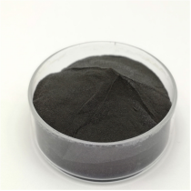
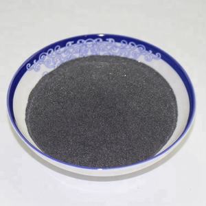
TRUNNANO jẹ olupilẹṣẹ Molybdenum Disulfide ti a mọ ni kariaye ati olupese ti awọn agbo ogun pẹlu diẹ sii ju 12 ọdun ti ĭrìrĭ ni ga didara nanomaterials ati awọn miiran kemikali. Ile-iṣẹ n ṣe agbekalẹ ọpọlọpọ awọn ohun elo lulú ati awọn kemikali. Pese OEM iṣẹ. Ti o ba nilo Molybdenum Disulfide ti o ga julọ, jọwọ lero free lati kan si wa. O le tẹ ọja naa lati kan si wa.
Awọn afi: Molybdenum Disulfide, nano molybdenum disulfide, MoS2
Gbogbo awọn nkan ati awọn aworan wa lati Intanẹẹti. Ti o ba wa eyikeyi awọn ọran aṣẹ lori ara, jọwọ kan si wa ni akoko lati parẹ.
Beere wa