


1. Кристалл рамкаһы һәм ярылған анизотропия
1.1 2Н һәм 1Т полиморфтары: Архитектура һәм һанлы икелек
(Молибден дисульфиды)
Молибден дисульфиды (MoS ₂) is a split shift metal dichalcogenide (ТМД) with a chemical formula consisting of one molybdenum atom sandwiched between 2 sulfur atoms in a trigonal prismatic sychronisation, ковалент бәйләнешле S барлыҡҡа килтерә.– Мо– S биттәре.
These private monolayers are stacked up and down and held with each other by weak van der Waals pressures, enabling simple interlayer shear and exfoliation to atomically slim two-dimensional (2D) кристалдар– a structural feature main to its diverse functional roles.
MoS two exists in several polymorphic kinds, the most thermodynamically secure being the semiconducting 2H phase (hexagonal balance), унда һәр ҡатлам тура диапазон арауығын күрһәтә ~ 1.8 туранан-тура диапазон арауығына күскән бер ҡатламлы типтағы эВ (~ 1.3 эВ) in bulk, a sensation critical for optoelectronic applications.
Икенсе яҡтан ., метастабиль 1Т фазаһы (tetragonal proportion) embraces an octahedral sychronisation and behaves as a metal conductor due to electron donation from the sulfur atoms, enabling applications in electrocatalysis and conductive composites.
Phase changes in between 2H and 1T can be induced chemically, электрохимик яҡтан, or via stress design, supplying a tunable system for creating multifunctional devices.
The capacity to support and pattern these phases spatially within a solitary flake opens up pathways for in-plane heterostructures with distinct electronic domains.
1.2 Етешһеҙлектәр, Допинг, һәм ян дәүләттәр
The efficiency of MoS two in catalytic and digital applications is extremely sensitive to atomic-scale issues and dopants.
Inherent point flaws such as sulfur jobs serve as electron donors, raising n-type conductivity and acting as active websites for hydrogen development responses (УНЫ) һыу ярыуҙа.
Grain borders and line problems can either hamper cost transport or develop localized conductive paths, depending on their atomic setup.
Regulated doping with shift steels (мәҫ., Тағы, Nb) йәки халкогендар (мәҫ., Se) enables fine-tuning of the band structure, service provider concentration, and spin-orbit coupling results.
Һис шикһеҙ, the edges of MoS two nanosheets, specifically the metal Mo-terminated (10– 10) sides, show dramatically higher catalytic activity than the inert basal airplane, motivating the layout of nanostructured drivers with made best use of edge direct exposure.
( Молибден дисульфиды)
These defect-engineered systems exemplify exactly how atomic-level manipulation can change a naturally occurring mineral right into a high-performance useful product.
2. Синтез һәм нанофабрикация стратегиялары
2.1 Bulk and Thin-Film Manufacturing Techniques
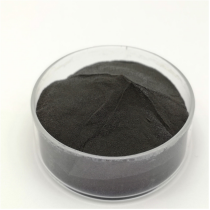
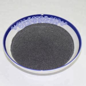
Тәбиғи молибденит, the mineral type of MoS ₂, has been utilized for years as a strong lubricant, however modern-day applications demand high-purity, structurally controlled artificial forms.
Химик пар менән ултыртыу (Йөрәк-йөрәк ауырыуы) is the dominant technique for creating large-area, high-crystallinity monolayer and few-layer MoS ₂ movies on substrates such as SiO TWO/ Si, сапфир, or flexible polymers.
СВД-ла, молибден һәм көкөрт прекурсорҙары (мәҫ., MoO дүрт һәм S порошок) are evaporated at heats (700– 1000 ° С )in control atmospheres, making it possible for layer-by-layer growth with tunable domain size and orientation.
Mechanical peeling (“скотч алымы”) stays a standard for research-grade examples, генерациялау ультра-таҙа моноҡатламдар менән маргиналь етешһеҙлектәр, масштаблылығы булмаһа ла.
Һыулы фазалы пилинг, including sonication or shear mixing of bulk crystals in solvents or surfactant remedies, produces colloidal dispersions of few-layer nanosheets suitable for layers, compounds, һәм буяу формулировкалары.
2.2 Heterostructure Assimilation and Tool Patterning
Real possibility of MoS ₂ arises when incorporated right into vertical or side heterostructures with other 2D materials such as graphene, алты мөйөшлө бор нитриды (h-BN), or WSe two.
These van der Waals heterostructures make it possible for the design of atomically precise gadgets, consisting of tunneling transistors, фотодетекторҙар, һәм яҡтылыҡ диодтары (Яҡтылыҡ диодтары), where interlayer charge and power transfer can be crafted.
Lithographic patterning and etching methods enable the manufacture of nanoribbons, квант нөктәләре, һәм ялан эффектлы транзисторҙар (ТЭТ) with network lengths down to tens of nanometers.
Dielectric encapsulation with h-BN secures MoS ₂ from ecological destruction and decreases charge scattering, substantially improving provider movement and gadget stability.
These manufacture breakthroughs are vital for transitioning MoS ₂ from lab interest to feasible part in next-generation nanoelectronics.
3. Functional Characteristics and Physical Mechanisms
3.1 Tribological Habits and Solid Lubrication
Among the oldest and most enduring applications of MoS two is as a dry solid lube in extreme atmospheres where liquid oils fail– саң һурҙырғыс кеүек, high temperatures, or cryogenic problems.
The reduced interlayer shear stamina of the van der Waals space enables simple sliding between S– Мо– S ҡатламдары, 0,03 тиклем кәметелгән һөртөү коэффициенты сәбәпсе була.– 0.06 under optimum conditions.
Its performance is further boosted by solid adhesion to steel surfaces and resistance to oxidation up to ~ 350 °С һауала, beyond which MoO ₃ formation increases wear.
MoS ₂ is commonly made use of in aerospace systems, vacuum pumps, and firearm parts, typically used as a covering via burnishing, һибеү, йәки полимер матрицаларға композит берләштереү.
Current researches show that moisture can degrade lubricity by boosting interlayer adhesion, motivating study right into hydrophobic layers or crossbreed lubricating substances for better environmental security.
3.2 Digital and Optoelectronic Reaction
As a direct-gap semiconductor in monolayer form, MoS ₂ exhibits strong light-matter communication, һеңдереү коэффициенттары 100-ҙән артыҡ булғанда. 10 ⁵ centimeters ⁻¹ and high quantum yield in photoluminescence.
This makes it excellent for ultrathin photodetectors with quick reaction times and broadband sensitivity, күренгән тулҡындарҙан яҡын инфраҡыҙыл тулҡындарға тиклем.
Field-effect transistors based upon monolayer MoS two demonstrate on/off proportions > 10 eight and service provider flexibilities approximately 500 centimeters ²/ V · s in suspended samples, though substrate communications normally limit practical worths to 1– 20 см ИКЕ/ В · с.
Спин-үҙән берләштереү, a repercussion of solid spin-orbit interaction and busted inversion proportion, makes it possible for valleytronics– an unique standard for info inscribing making use of the valley degree of liberty in energy room.
These quantum sensations position MoS ₂ as a candidate for low-power logic, хәтер, and quantum computer elements.
4. Ҡулланыу ҡөҙрәте, Катализ, and Arising Technologies
4.1 Electrocatalysis for Hydrogen Advancement Response (УНЫ)
MoS two has actually become an encouraging non-precious alternative to platinum in the hydrogen advancement response (УНЫ), an essential process in water electrolysis for environment-friendly hydrogen production.
While the basic plane is catalytically inert, edge sites and sulfur jobs display near-optimal hydrogen adsorption totally free energy (ДГ_Н * ≈ 0), comparable to Pt.
Nanostructuring methods– such as creating vertically straightened nanosheets, defect-rich films, or doped hybrids with Ni or Co– take full advantage of active site thickness and electrical conductivity.
When incorporated into electrodes with conductive sustains like carbon nanotubes or graphene, MoS two attains high present thickness and lasting security under acidic or neutral conditions.
More enhancement is accomplished by maintaining the metal 1T stage, which boosts intrinsic conductivity and reveals additional active sites.
4.2 Adaptable Electronics, Датчиктар, һәм квант ҡоролмалары
The mechanical versatility, openness, and high surface-to-volume proportion of MoS two make it ideal for flexible and wearable electronics.
Транзисторҙар, логик схемалар, and memory gadgets have been demonstrated on plastic substratums, enabling bendable display screens, һаулыҡ күрһәтеү, and IoT sensors.
MoS ₂-based gas sensors display high sensitivity to NO ₂, NH THREE, and H TWO O due to bill transfer upon molecular adsorption, with feedback times in the sub-second variety.
Квант заманса технологияларҙа, MoS ₂ hosts localized excitons and trions at cryogenic temperature levels, and strain-induced pseudomagnetic areas can trap service providers, allowing single-photon emitters and quantum dots.
These growths highlight MoS two not just as a useful material however as a system for exploring essential physics in decreased dimensions.
Йомғаҡлап, molybdenum disulfide exemplifies the merging of classical products scientific research and quantum design.
From its ancient role as a lubricating substance to its modern deployment in atomically thin electronic devices and power systems, MoS two continues to redefine the borders of what is feasible in nanoscale materials design.
Синтез булараҡ, характеристика биреү, and assimilation methods development, its impact throughout scientific research and modern technology is positioned to expand even further.
5. Дистрибьютор
TRUNNANO — донъя кимәлендә танылған молибден дисульфиды етештереүсе һәм тәьмин итеүсе берләшмәләр менән күберәк 12 Юғары сифатлы наноматериалдар һәм башҡа химик матдәләр буйынса 10 йыл экспертиза. Компания төрлө порошок материалдар һәм химик матдәләр эшләй .. OEM хеҙмәте күрһәтеү. Әгәр һеҙгә кәрәк юғары сифатлы молибден дисульфид, рәхим итеп, беҙҙең менән бәйләнешкә инегеҙ. Һеҙ беҙҙең менән бәйләнешкә инеү өсөн продукт баҫып була ..
Тегтар: Молибден дисульфиды, нано молибден дисульфиды, МОС2.
Бөтә мәҡәләләр һәм һүрәттәр интернеттан алынған .. Әгәр ниндәй ҙә булһа авторлыҡ хоҡуғы мәсьәләләре, зинһар, беҙҙең менән бәйләнешкә инеү өсөн ваҡытында юйырға.
Беҙгә һорау бирегеҙ