


1. ਕ੍ਰਿਸਟਲ ਫਰੇਮਵਰਕ ਅਤੇ ਸਪਲਿਟ ਐਨੀਸੋਟ੍ਰੋਪੀ
1.1 2H ਅਤੇ 1T ਪੋਲੀਮੋਰਫਸ: ਆਰਕੀਟੈਕਚਰਲ ਅਤੇ ਡਿਜੀਟਲ ਡਿਊਲਿਟੀ
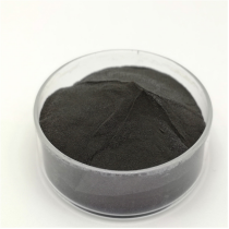
(ਮੋਲੀਬਡੇਨਮ ਡਿਸਲਫਾਈਡ)
ਮੋਲੀਬਡੇਨਮ ਡਿਸਲਫਾਈਡ (ਰਾਜ ਮੰਤਰੀ ₂) ਇੱਕ ਸਪਲਿਟ ਸ਼ਿਫਟ ਮੈਟਲ ਡਾਇਕਲਕੋਜੀਨਾਈਡ ਹੈ (ਟੀ.ਐਮ.ਡੀ) ਇੱਕ ਰਸਾਇਣਕ ਫਾਰਮੂਲੇ ਦੇ ਨਾਲ ਜਿਸ ਵਿੱਚ ਇੱਕ ਮੋਲੀਬਡੇਨਮ ਐਟਮ ਸੈਂਡਵਿਚ ਹੁੰਦਾ ਹੈ 2 ਇੱਕ ਤਿਕੋਣੀ ਪ੍ਰਿਜ਼ਮੈਟਿਕ ਸਿਕ੍ਰੋਨਾਈਜ਼ੇਸ਼ਨ ਵਿੱਚ ਗੰਧਕ ਦੇ ਪਰਮਾਣੂ, covalently bonded S ਬਣਾਉਣਾ– ਮੋ– ਐਸ ਸ਼ੀਟਾਂ.
ਇਹ ਨਿਜੀ ਮੋਨੋਲੇਅਰ ਉੱਪਰ ਅਤੇ ਹੇਠਾਂ ਸਟੈਕ ਕੀਤੇ ਜਾਂਦੇ ਹਨ ਅਤੇ ਕਮਜ਼ੋਰ ਵੈਨ ਡੇਰ ਵਾਲਜ਼ ਦਬਾਅ ਦੁਆਰਾ ਇੱਕ ਦੂਜੇ ਨਾਲ ਫੜੇ ਜਾਂਦੇ ਹਨ, ਪਰਮਾਣੂ ਤੌਰ 'ਤੇ ਪਤਲੇ ਦੋ-ਅਯਾਮੀ ਲਈ ਸਧਾਰਨ ਇੰਟਰਲੇਅਰ ਸ਼ੀਅਰ ਅਤੇ ਐਕਸਫੋਲੀਏਸ਼ਨ ਨੂੰ ਸਮਰੱਥ ਬਣਾਉਣਾ (2ਡੀ) ਕ੍ਰਿਸਟਲ– ਇੱਕ ਢਾਂਚਾਗਤ ਵਿਸ਼ੇਸ਼ਤਾ ਇਸ ਦੀਆਂ ਵਿਭਿੰਨ ਕਾਰਜਸ਼ੀਲ ਭੂਮਿਕਾਵਾਂ ਲਈ ਮੁੱਖ ਹੈ.
MoS ਦੋ ਕਈ ਪੌਲੀਮੋਰਫਿਕ ਕਿਸਮਾਂ ਵਿੱਚ ਮੌਜੂਦ ਹਨ, ਸਭ ਤੋਂ ਵੱਧ ਥਰਮੋਡਾਇਨਾਮਿਕ ਤੌਰ 'ਤੇ ਸੁਰੱਖਿਅਤ ਸੈਮੀਕੰਡਕਟਿੰਗ 2H ਪੜਾਅ ਹੈ (ਹੈਕਸਾਗੋਨਲ ਸੰਤੁਲਨ), ਜਿੱਥੇ ਹਰ ਪਰਤ ~ ਦਾ ਸਿੱਧਾ ਬੈਂਡਗੈਪ ਦਿਖਾਉਂਦੀ ਹੈ 1.8 ਮੋਨੋਲੇਅਰ ਕਿਸਮ ਵਿੱਚ eV ਜੋ ਇੱਕ ਅਸਿੱਧੇ ਬੈਂਡਗੈਪ ਵਿੱਚ ਬਦਲਦਾ ਹੈ (~ 1.3 eV) ਥੋਕ ਵਿੱਚ, ਆਪਟੋਇਲੈਕਟ੍ਰੌਨਿਕ ਐਪਲੀਕੇਸ਼ਨਾਂ ਲਈ ਇੱਕ ਸੰਵੇਦਨਾ ਨਾਜ਼ੁਕ.
ਦੂਜੇ ਹਥ੍ਥ ਤੇ, ਮੈਟਾਸਟੇਬਲ 1T ਪੜਾਅ (ਟੈਟਰਾਗੋਨਲ ਅਨੁਪਾਤ) ਗੰਧਕ ਦੇ ਪਰਮਾਣੂਆਂ ਤੋਂ ਇਲੈਕਟ੍ਰੋਨ ਦਾਨ ਦੇ ਕਾਰਨ ਇੱਕ ਅਸ਼ਟੈਡ੍ਰਲ ਸਿਕ੍ਰੋਨਾਈਜ਼ੇਸ਼ਨ ਨੂੰ ਗਲੇ ਲੈਂਦਾ ਹੈ ਅਤੇ ਇੱਕ ਧਾਤ ਦੇ ਕੰਡਕਟਰ ਵਜੋਂ ਵਿਹਾਰ ਕਰਦਾ ਹੈ, ਇਲੈਕਟ੍ਰੋਕੈਟਾਲਿਸਿਸ ਅਤੇ ਸੰਚਾਲਕ ਕੰਪੋਜ਼ਿਟਸ ਵਿੱਚ ਐਪਲੀਕੇਸ਼ਨਾਂ ਨੂੰ ਸਮਰੱਥ ਬਣਾਉਣਾ.
2H ਅਤੇ 1T ਦੇ ਵਿਚਕਾਰ ਪੜਾਅ ਵਿੱਚ ਤਬਦੀਲੀਆਂ ਨੂੰ ਰਸਾਇਣਕ ਤੌਰ 'ਤੇ ਪ੍ਰੇਰਿਤ ਕੀਤਾ ਜਾ ਸਕਦਾ ਹੈ, ਇਲੈਕਟ੍ਰੋਕੈਮਿਕ ਤੌਰ 'ਤੇ, ਜਾਂ ਤਣਾਅ ਡਿਜ਼ਾਈਨ ਦੁਆਰਾ, ਮਲਟੀਫੰਕਸ਼ਨਲ ਡਿਵਾਈਸਾਂ ਬਣਾਉਣ ਲਈ ਇੱਕ ਟਿਊਨੇਬਲ ਸਿਸਟਮ ਦੀ ਸਪਲਾਈ ਕਰਨਾ.
ਇਨ੍ਹਾਂ ਪੜਾਵਾਂ ਨੂੰ ਇਕਾਂਤ ਫਲੇਕ ਦੇ ਅੰਦਰ ਸਥਾਨਿਕ ਤੌਰ 'ਤੇ ਸਮਰਥਨ ਅਤੇ ਪੈਟਰਨ ਕਰਨ ਦੀ ਸਮਰੱਥਾ ਵੱਖਰੇ ਇਲੈਕਟ੍ਰਾਨਿਕ ਡੋਮੇਨਾਂ ਦੇ ਨਾਲ ਇਨ-ਪਲੇਨ ਹੇਟਰੋਸਟ੍ਰਕਚਰ ਲਈ ਮਾਰਗ ਖੋਲ੍ਹਦੀ ਹੈ।.
1.2 ਨੁਕਸ, ਡੋਪਿੰਗ, ਅਤੇ ਪਾਸੇ ਦੇ ਰਾਜ
ਉਤਪ੍ਰੇਰਕ ਅਤੇ ਡਿਜੀਟਲ ਐਪਲੀਕੇਸ਼ਨਾਂ ਵਿੱਚ ਐਮਓਐਸ ਦੋ ਦੀ ਕੁਸ਼ਲਤਾ ਪਰਮਾਣੂ-ਪੈਮਾਨੇ ਦੇ ਮੁੱਦਿਆਂ ਅਤੇ ਡੋਪੈਂਟਸ ਲਈ ਬਹੁਤ ਸੰਵੇਦਨਸ਼ੀਲ ਹੈ.
ਅੰਦਰੂਨੀ ਬਿੰਦੂ ਖਾਮੀਆਂ ਜਿਵੇਂ ਕਿ ਗੰਧਕ ਦੀਆਂ ਨੌਕਰੀਆਂ ਇਲੈਕਟ੍ਰੌਨ ਦਾਨੀ ਵਜੋਂ ਕੰਮ ਕਰਦੀਆਂ ਹਨ, n-ਕਿਸਮ ਦੀ ਚਾਲਕਤਾ ਨੂੰ ਵਧਾਉਣਾ ਅਤੇ ਹਾਈਡ੍ਰੋਜਨ ਵਿਕਾਸ ਪ੍ਰਤੀਕ੍ਰਿਆਵਾਂ ਲਈ ਸਰਗਰਮ ਵੈਬਸਾਈਟਾਂ ਵਜੋਂ ਕੰਮ ਕਰਨਾ (ਉਸ ਨੂੰ) ਪਾਣੀ ਵੰਡਣ ਵਿੱਚ.
ਅਨਾਜ ਦੀਆਂ ਸਰਹੱਦਾਂ ਅਤੇ ਲਾਈਨ ਦੀਆਂ ਸਮੱਸਿਆਵਾਂ ਜਾਂ ਤਾਂ ਲਾਗਤ ਦੀ ਆਵਾਜਾਈ ਨੂੰ ਰੋਕ ਸਕਦੀਆਂ ਹਨ ਜਾਂ ਸਥਾਨਕ ਸੰਚਾਲਕ ਮਾਰਗ ਵਿਕਸਿਤ ਕਰ ਸਕਦੀਆਂ ਹਨ, ਆਪਣੇ ਪਰਮਾਣੂ ਸੈੱਟਅੱਪ 'ਤੇ ਨਿਰਭਰ ਕਰਦਾ ਹੈ.
ਸ਼ਿਫਟ ਸਟੀਲਜ਼ ਨਾਲ ਨਿਯੰਤ੍ਰਿਤ ਡੋਪਿੰਗ (ਜਿਵੇਂ ਕਿ, ਰੀ, ਐਨ.ਬੀ) ਜਾਂ ਚੈਲਕੋਜਨ (ਜਿਵੇਂ ਕਿ, ਸੇ) ਬੈਂਡ ਬਣਤਰ ਦੀ ਵਧੀਆ ਟਿਊਨਿੰਗ ਨੂੰ ਸਮਰੱਥ ਬਣਾਉਂਦਾ ਹੈ, ਸੇਵਾ ਪ੍ਰਦਾਤਾ ਇਕਾਗਰਤਾ, ਅਤੇ ਸਪਿਨ-ਔਰਬਿਟ ਕਪਲਿੰਗ ਨਤੀਜੇ.
ਮਹੱਤਵਪੂਰਨ ਤੌਰ 'ਤੇ, MoS ਦੋ ਨੈਨੋਸ਼ੀਟਾਂ ਦੇ ਕਿਨਾਰੇ, ਖਾਸ ਤੌਰ 'ਤੇ ਮੋ-ਟਰਮੀਨੇਟਡ ਧਾਤ (10– 10) ਪਾਸੇ, ਇਨਰਟ ਬੇਸਲ ਏਅਰਪਲੇਨ ਨਾਲੋਂ ਨਾਟਕੀ ਤੌਰ 'ਤੇ ਉੱਚ ਉਤਪ੍ਰੇਰਕ ਗਤੀਵਿਧੀ ਦਿਖਾਓ, ਕਿਨਾਰੇ ਦੇ ਸਿੱਧੇ ਐਕਸਪੋਜ਼ਰ ਦੀ ਵਧੀਆ ਵਰਤੋਂ ਨਾਲ ਨੈਨੋਸਟ੍ਰਕਚਰਡ ਡਰਾਈਵਰਾਂ ਦੇ ਖਾਕੇ ਨੂੰ ਪ੍ਰੇਰਿਤ ਕਰਨਾ.
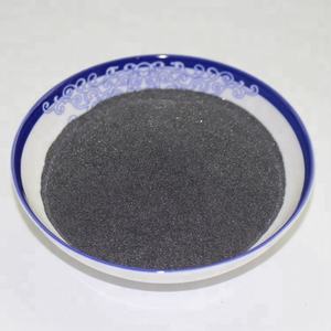
( ਮੋਲੀਬਡੇਨਮ ਡਿਸਲਫਾਈਡ)
ਇਹ ਨੁਕਸ-ਇੰਜੀਨੀਅਰ ਸਿਸਟਮ ਬਿਲਕੁਲ ਉਦਾਹਰਣ ਦਿੰਦੇ ਹਨ ਕਿ ਕਿਵੇਂ ਪ੍ਰਮਾਣੂ-ਪੱਧਰ ਦੀ ਹੇਰਾਫੇਰੀ ਕੁਦਰਤੀ ਤੌਰ 'ਤੇ ਹੋਣ ਵਾਲੇ ਖਣਿਜ ਨੂੰ ਉੱਚ-ਪ੍ਰਦਰਸ਼ਨ ਲਾਭਦਾਇਕ ਉਤਪਾਦ ਵਿੱਚ ਬਦਲ ਸਕਦੀ ਹੈ।.
2. ਸੰਸਲੇਸ਼ਣ ਅਤੇ ਨੈਨੋਫੈਬਰੀਕੇਸ਼ਨ ਰਣਨੀਤੀਆਂ
2.1 ਬਲਕ ਅਤੇ ਥਿਨ-ਫਿਲਮ ਨਿਰਮਾਣ ਤਕਨੀਕਾਂ
ਕੁਦਰਤੀ ਮੋਲੀਬਡੇਨਾਈਟ, MoS ₂ ਦੀ ਖਣਿਜ ਕਿਸਮ, ਇੱਕ ਮਜ਼ਬੂਤ ਲੁਬਰੀਕੈਂਟ ਵਜੋਂ ਸਾਲਾਂ ਤੋਂ ਵਰਤਿਆ ਗਿਆ ਹੈ, ਹਾਲਾਂਕਿ ਆਧੁਨਿਕ-ਦਿਨ ਦੀਆਂ ਐਪਲੀਕੇਸ਼ਨਾਂ ਉੱਚ-ਸ਼ੁੱਧਤਾ ਦੀ ਮੰਗ ਕਰਦੀਆਂ ਹਨ, ਢਾਂਚਾਗਤ ਤੌਰ 'ਤੇ ਨਿਯੰਤਰਿਤ ਨਕਲੀ ਰੂਪ.
ਰਸਾਇਣਕ ਭਾਫ਼ ਜਮ੍ਹਾ (ਸੀਵੀਡੀ) ਵੱਡੇ ਖੇਤਰ ਨੂੰ ਬਣਾਉਣ ਲਈ ਪ੍ਰਮੁੱਖ ਤਕਨੀਕ ਹੈ, ਸਬਸਟਰੇਟਾਂ ਜਿਵੇਂ ਕਿ SiO TWO/ Si 'ਤੇ ਉੱਚ-ਕ੍ਰਿਸਟਲਿਨਿਟੀ ਮੋਨੋਲੇਅਰ ਅਤੇ ਕੁਝ-ਲੇਅਰ MoS ₂ ਫਿਲਮਾਂ, ਨੀਲਮ, ਜਾਂ ਲਚਕਦਾਰ ਪੌਲੀਮਰ.
CVD ਵਿੱਚ, ਮੋਲੀਬਡੇਨਮ ਅਤੇ ਗੰਧਕ ਦੇ ਪੂਰਵਜ (ਜਿਵੇਂ ਕਿ, MoO ਚਾਰ ਅਤੇ S ਪਾਊਡਰ) ਗਰਮੀ 'ਤੇ ਭਾਫ਼ ਬਣ ਜਾਂਦੇ ਹਨ (700– 1000 ° ਸੈਂ )ਕੰਟਰੋਲ ਵਾਯੂਮੰਡਲ ਵਿੱਚ, ਟਿਊਨੇਬਲ ਡੋਮੇਨ ਆਕਾਰ ਅਤੇ ਸਥਿਤੀ ਦੇ ਨਾਲ ਲੇਅਰ-ਦਰ-ਲੇਅਰ ਵਿਕਾਸ ਨੂੰ ਸੰਭਵ ਬਣਾਉਂਦਾ ਹੈ.
ਮਕੈਨੀਕਲ ਛਿੱਲ (“ਸਕਾਚ ਟੇਪ ਪਹੁੰਚ”) ਖੋਜ-ਗਰੇਡ ਉਦਾਹਰਨਾਂ ਲਈ ਇੱਕ ਮਿਆਰ ਬਣਿਆ ਰਹਿੰਦਾ ਹੈ, ਮਾਮੂਲੀ ਖਾਮੀਆਂ ਦੇ ਨਾਲ ਅਲਟਰਾ-ਕਲੀਨ ਮੋਨੋਲੇਅਰ ਤਿਆਰ ਕਰਨਾ, ਹਾਲਾਂਕਿ ਇਸ ਵਿੱਚ ਮਾਪਯੋਗਤਾ ਨਹੀਂ ਹੈ.
ਤਰਲ-ਪੜਾਅ ਪੀਲਿੰਗ, ਸੌਲਵੈਂਟਸ ਜਾਂ ਸਰਫੈਕਟੈਂਟ ਉਪਚਾਰਾਂ ਵਿੱਚ ਬਲਕ ਕ੍ਰਿਸਟਲ ਦੀ ਸੋਨਿਕੇਸ਼ਨ ਜਾਂ ਸ਼ੀਅਰ ਮਿਕਸਿੰਗ ਸਮੇਤ, ਲੇਅਰਾਂ ਲਈ ਢੁਕਵੀਂ ਕੁਝ-ਲੇਅਰ ਨੈਨੋਸ਼ੀਟਾਂ ਦੇ ਕੋਲੋਇਡਲ ਫੈਲਾਅ ਪੈਦਾ ਕਰਦਾ ਹੈ, ਮਿਸ਼ਰਣ, ਅਤੇ ਸਿਆਹੀ ਦੇ ਫਾਰਮੂਲੇ.
2.2 ਹੇਟਰੋਸਟ੍ਰਕਚਰ ਐਸੀਮੀਲੇਸ਼ਨ ਅਤੇ ਟੂਲ ਪੈਟਰਨਿੰਗ
MoS ₂ ਦੀ ਅਸਲ ਸੰਭਾਵਨਾ ਉਦੋਂ ਪੈਦਾ ਹੁੰਦੀ ਹੈ ਜਦੋਂ ਗ੍ਰਾਫੀਨ ਵਰਗੀਆਂ ਹੋਰ 2D ਸਮੱਗਰੀਆਂ ਦੇ ਨਾਲ ਵਰਟੀਕਲ ਜਾਂ ਸਾਈਡ ਹੇਟਰੋਸਟ੍ਰਕਚਰ ਵਿੱਚ ਸ਼ਾਮਲ ਕੀਤਾ ਜਾਂਦਾ ਹੈ, ਹੈਕਸਾਗੋਨਲ ਬੋਰਾਨ ਨਾਈਟ੍ਰਾਈਡ (h-BN), ਜਾਂ ਦੋ ਡਬਲਯੂ.
ਇਹ ਵੈਨ ਡੇਰ ਵਾਲਸ ਹੈਟਰੋਸਟ੍ਰਕਚਰ ਪਰਮਾਣੂ ਤੌਰ 'ਤੇ ਸਟੀਕ ਯੰਤਰਾਂ ਦੇ ਡਿਜ਼ਾਈਨ ਨੂੰ ਸੰਭਵ ਬਣਾਉਂਦੇ ਹਨ।, ਟਨਲਿੰਗ ਟਰਾਂਜ਼ਿਸਟਰਾਂ ਦੇ ਸ਼ਾਮਲ ਹਨ, ਫੋਟੋ ਡਿਟੈਕਟਰ, ਅਤੇ ਲਾਈਟ-ਐਮੀਟਿੰਗ ਡਾਇਡਸ (ਐਲ.ਈ.ਡੀ), ਜਿੱਥੇ ਇੰਟਰਲੇਅਰ ਚਾਰਜ ਅਤੇ ਪਾਵਰ ਟ੍ਰਾਂਸਫਰ ਨੂੰ ਤਿਆਰ ਕੀਤਾ ਜਾ ਸਕਦਾ ਹੈ.
ਲਿਥੋਗ੍ਰਾਫਿਕ ਪੈਟਰਨਿੰਗ ਅਤੇ ਐਚਿੰਗ ਵਿਧੀਆਂ ਨੈਨੋਰੀਬਨ ਦੇ ਨਿਰਮਾਣ ਨੂੰ ਸਮਰੱਥ ਬਣਾਉਂਦੀਆਂ ਹਨ, ਕੁਆਂਟਮ ਬਿੰਦੀਆਂ, ਅਤੇ ਫੀਲਡ-ਇਫੈਕਟ ਟਰਾਂਜ਼ਿਸਟਰ (FETs) ਨੈੱਟਵਰਕ ਦੀ ਲੰਬਾਈ ਨੈਨੋਮੀਟਰ ਦੇ ਦਸਾਂ ਤੱਕ ਘੱਟ ਹੈ.
ਐਚ-ਬੀਐਨ ਦੇ ਨਾਲ ਡਾਈਇਲੈਕਟ੍ਰਿਕ ਇਨਕੈਪਸੂਲੇਸ਼ਨ ਐਮਓਐਸ ₂ ਨੂੰ ਵਾਤਾਵਰਣਿਕ ਵਿਨਾਸ਼ ਤੋਂ ਸੁਰੱਖਿਅਤ ਕਰਦਾ ਹੈ ਅਤੇ ਚਾਰਜ ਸਕੈਟਰਿੰਗ ਨੂੰ ਘਟਾਉਂਦਾ ਹੈ, ਪ੍ਰਦਾਤਾ ਦੀ ਗਤੀ ਅਤੇ ਗੈਜੇਟ ਸਥਿਰਤਾ ਵਿੱਚ ਕਾਫ਼ੀ ਸੁਧਾਰ ਕਰਨਾ.
ਇਹ ਨਿਰਮਾਣ ਸਫਲਤਾਵਾਂ ਅਗਲੀ ਪੀੜ੍ਹੀ ਦੇ ਨੈਨੋਇਲੈਕਟ੍ਰੋਨਿਕਸ ਵਿੱਚ ਲੈਬ ਦਿਲਚਸਪੀ ਤੋਂ ਵਿਹਾਰਕ ਹਿੱਸੇ ਤੱਕ MoS ₂ ਨੂੰ ਬਦਲਣ ਲਈ ਮਹੱਤਵਪੂਰਨ ਹਨ।.
3. ਕਾਰਜਸ਼ੀਲ ਵਿਸ਼ੇਸ਼ਤਾਵਾਂ ਅਤੇ ਭੌਤਿਕ ਵਿਧੀਆਂ
3.1 ਟ੍ਰਾਈਬੋਲੋਜੀਕਲ ਆਦਤਾਂ ਅਤੇ ਠੋਸ ਲੁਬਰੀਕੇਸ਼ਨ
MoS ਦੋ ਦੇ ਸਭ ਤੋਂ ਪੁਰਾਣੇ ਅਤੇ ਸਭ ਤੋਂ ਵੱਧ ਸਥਾਈ ਉਪਯੋਗਾਂ ਵਿੱਚੋਂ ਇੱਕ ਬਹੁਤ ਜ਼ਿਆਦਾ ਵਾਯੂਮੰਡਲ ਵਿੱਚ ਇੱਕ ਸੁੱਕੀ ਠੋਸ ਲੂਬ ਹੈ ਜਿੱਥੇ ਤਰਲ ਤੇਲ ਅਸਫਲ ਹੋ ਜਾਂਦੇ ਹਨ– ਜਿਵੇਂ ਕਿ ਵੈਕਿਊਮ ਕਲੀਨਰ, ਉੱਚ ਤਾਪਮਾਨ, ਜਾਂ ਕ੍ਰਾਇਓਜੇਨਿਕ ਸਮੱਸਿਆਵਾਂ.
ਵੈਨ ਡੇਰ ਵਾਲਸ ਸਪੇਸ ਦੀ ਘਟੀ ਹੋਈ ਇੰਟਰਲੇਅਰ ਸ਼ੀਅਰ ਸਟੈਮਿਨਾ S ਵਿਚਕਾਰ ਸਧਾਰਣ ਸਲਾਈਡਿੰਗ ਨੂੰ ਸਮਰੱਥ ਬਣਾਉਂਦੀ ਹੈ– ਮੋ– S ਲੇਅਰਾਂ, 0.03 ਦੇ ਰੂਪ ਵਿੱਚ ਘਟਾ ਕੇ ਰਗੜਨ ਦੇ ਗੁਣਾਂ ਦਾ ਕਾਰਨ ਬਣ ਰਿਹਾ ਹੈ– 0.06 ਸਰਵੋਤਮ ਹਾਲਾਤ ਦੇ ਤਹਿਤ.
ਇਸਦੀ ਕਾਰਜਕੁਸ਼ਲਤਾ ਨੂੰ ਸਟੀਲ ਦੀਆਂ ਸਤਹਾਂ ਦੇ ਠੋਸ ਚਿਪਕਣ ਅਤੇ ~ ਤੱਕ ਆਕਸੀਕਰਨ ਦੇ ਪ੍ਰਤੀਰੋਧ ਦੁਆਰਾ ਅੱਗੇ ਵਧਾਇਆ ਗਿਆ ਹੈ 350 ਹਵਾ ਵਿੱਚ °C, ਜਿਸ ਤੋਂ ਪਰੇ MoO ₃ ਗਠਨ ਪਹਿਨਣ ਨੂੰ ਵਧਾਉਂਦਾ ਹੈ.
MoS ₂ ਦੀ ਆਮ ਤੌਰ 'ਤੇ ਏਰੋਸਪੇਸ ਪ੍ਰਣਾਲੀਆਂ ਵਿੱਚ ਵਰਤੋਂ ਕੀਤੀ ਜਾਂਦੀ ਹੈ, ਵੈਕਿਊਮ ਪੰਪ, ਅਤੇ ਹਥਿਆਰਾਂ ਦੇ ਹਿੱਸੇ, ਆਮ ਤੌਰ 'ਤੇ ਬਰਨਿਸ਼ਿੰਗ ਦੁਆਰਾ ਇੱਕ ਢੱਕਣ ਵਜੋਂ ਵਰਤਿਆ ਜਾਂਦਾ ਹੈ, ਥੁੱਕਣਾ, ਜਾਂ ਪੌਲੀਮਰ ਮੈਟ੍ਰਿਕਸ ਵਿੱਚ ਸੰਯੁਕਤ ਏਕੀਕਰਨ.
ਮੌਜੂਦਾ ਖੋਜਾਂ ਦਰਸਾਉਂਦੀਆਂ ਹਨ ਕਿ ਨਮੀ ਇੰਟਰਲੇਅਰ ਅਡਜਸ਼ਨ ਨੂੰ ਵਧਾ ਕੇ ਲੁਬਰੀਸਿਟੀ ਨੂੰ ਘਟਾ ਸਕਦੀ ਹੈ, ਬਿਹਤਰ ਵਾਤਾਵਰਣ ਸੁਰੱਖਿਆ ਲਈ ਹਾਈਡ੍ਰੋਫੋਬਿਕ ਪਰਤਾਂ ਜਾਂ ਕਰਾਸਬ੍ਰੀਡ ਲੁਬਰੀਕੇਟਿੰਗ ਪਦਾਰਥਾਂ ਵਿੱਚ ਅਧਿਐਨ ਨੂੰ ਪ੍ਰੇਰਿਤ ਕਰਨਾ.
3.2 ਡਿਜੀਟਲ ਅਤੇ ਆਪਟੋਇਲੈਕਟ੍ਰੋਨਿਕ ਪ੍ਰਤੀਕਿਰਿਆ
ਮੋਨੋਲਾਇਰ ਰੂਪ ਵਿੱਚ ਇੱਕ ਡਾਇਰੈਕਟ-ਗੈਪ ਸੈਮੀਕੰਡਕਟਰ ਵਜੋਂ, MoS ₂ ਮਜ਼ਬੂਤ ਲਾਈਟ-ਮੈਟਰ ਸੰਚਾਰ ਪ੍ਰਦਰਸ਼ਿਤ ਕਰਦਾ ਹੈ, ਤੋਂ ਵੱਧ ਸਮਾਈ ਗੁਣਾਂਕ ਦੇ ਨਾਲ 10 ⁵ ਸੈਂਟੀਮੀਟਰ ⁻¹ ਅਤੇ ਫੋਟੋਲੁਮਿਨਿਸੈਂਸ ਵਿੱਚ ਉੱਚ ਕੁਆਂਟਮ ਉਪਜ.
ਇਹ ਤੇਜ਼ ਪ੍ਰਤੀਕ੍ਰਿਆ ਦੇ ਸਮੇਂ ਅਤੇ ਬ੍ਰੌਡਬੈਂਡ ਸੰਵੇਦਨਸ਼ੀਲਤਾ ਵਾਲੇ ਅਲਟਰਾਥਿਨ ਫੋਟੋਡਿਟੈਕਟਰਾਂ ਲਈ ਸ਼ਾਨਦਾਰ ਬਣਾਉਂਦਾ ਹੈ, ਦ੍ਰਿਸ਼ਮਾਨ ਤੋਂ ਲੈ ਕੇ ਨੇੜੇ-ਇਨਫਰਾਰੈੱਡ ਤਰੰਗ-ਲੰਬਾਈ ਤੱਕ.
ਮੋਨੋਲੇਅਰ ਐਮਓਐਸ ਦੋ ਦੇ ਅਧਾਰ ਤੇ ਫੀਲਡ-ਇਫੈਕਟ ਟਰਾਂਜ਼ਿਸਟਰ ਚਾਲੂ/ਬੰਦ ਅਨੁਪਾਤ ਦਾ ਪ੍ਰਦਰਸ਼ਨ ਕਰਦੇ ਹਨ > 10 ਅੱਠ ਅਤੇ ਸੇਵਾ ਪ੍ਰਦਾਤਾ ਲਗਭਗ ਲਚਕਤਾ 500 ਮੁਅੱਤਲ ਕੀਤੇ ਨਮੂਨਿਆਂ ਵਿੱਚ ਸੈਂਟੀਮੀਟਰ ²/ V · s, ਹਾਲਾਂਕਿ ਸਬਸਟਰੇਟ ਸੰਚਾਰ ਆਮ ਤੌਰ 'ਤੇ ਵਿਹਾਰਕ ਮੁੱਲਾਂ ਨੂੰ 1 ਤੱਕ ਸੀਮਤ ਕਰਦੇ ਹਨ– 20 cm TWO/ V · s.
ਸਪਿਨ-ਵਾਦੀ ਸੰਯੋਗ, ਠੋਸ ਸਪਿੱਨ-ਔਰਬਿਟ ਪਰਸਪਰ ਕ੍ਰਿਆ ਅਤੇ ਪਰਦਾਫਾਸ਼ ਉਲਟ ਅਨੁਪਾਤ ਦਾ ਪ੍ਰਤੀਕਰਮ, ਵੈਲੀਟ੍ਰੋਨਿਕਸ ਲਈ ਇਸਨੂੰ ਸੰਭਵ ਬਣਾਉਂਦਾ ਹੈ– ਊਰਜਾ ਕਮਰੇ ਵਿੱਚ ਆਜ਼ਾਦੀ ਦੀ ਘਾਟੀ ਦੀ ਡਿਗਰੀ ਦੀ ਵਰਤੋਂ ਕਰਨ ਵਾਲੀ ਜਾਣਕਾਰੀ ਲਈ ਇੱਕ ਵਿਲੱਖਣ ਮਿਆਰ.
ਇਹ ਕੁਆਂਟਮ ਸੰਵੇਦਨਾਵਾਂ MoS ₂ ਨੂੰ ਘੱਟ-ਸ਼ਕਤੀ ਵਾਲੇ ਤਰਕ ਲਈ ਉਮੀਦਵਾਰ ਵਜੋਂ ਸਥਿਤੀ ਵਿੱਚ ਰੱਖਦੀਆਂ ਹਨ, ਮੈਮੋਰੀ, ਅਤੇ ਕੁਆਂਟਮ ਕੰਪਿਊਟਰ ਤੱਤ.
4. ਪਾਵਰ ਵਿੱਚ ਐਪਲੀਕੇਸ਼ਨ, ਉਤਪ੍ਰੇਰਕ, ਅਤੇ ਪੈਦਾ ਹੋਣ ਵਾਲੀਆਂ ਤਕਨਾਲੋਜੀਆਂ
4.1 ਹਾਈਡ੍ਰੋਜਨ ਐਡਵਾਂਸਮੈਂਟ ਰਿਸਪਾਂਸ ਲਈ ਇਲੈਕਟ੍ਰੋਕੈਟਾਲਿਸਿਸ (ਉਸ ਨੂੰ)
ਐਮਓਐਸ ਦੋ ਅਸਲ ਵਿੱਚ ਹਾਈਡ੍ਰੋਜਨ ਐਡਵਾਂਸਮੈਂਟ ਜਵਾਬ ਵਿੱਚ ਪਲੈਟੀਨਮ ਦਾ ਇੱਕ ਉਤਸ਼ਾਹਜਨਕ ਗੈਰ-ਕੀਮਤੀ ਵਿਕਲਪ ਬਣ ਗਿਆ ਹੈ (ਉਸ ਨੂੰ), ਵਾਤਾਵਰਣ-ਅਨੁਕੂਲ ਹਾਈਡ੍ਰੋਜਨ ਉਤਪਾਦਨ ਲਈ ਪਾਣੀ ਦੇ ਇਲੈਕਟ੍ਰੋਲਾਈਸਿਸ ਵਿੱਚ ਇੱਕ ਜ਼ਰੂਰੀ ਪ੍ਰਕਿਰਿਆ.
ਜਦੋਂ ਕਿ ਮੂਲ ਪਲੇਨ ਉਤਪ੍ਰੇਰਕ ਤੌਰ 'ਤੇ ਅੜਿੱਕਾ ਹੈ, ਕਿਨਾਰੇ ਵਾਲੀਆਂ ਸਾਈਟਾਂ ਅਤੇ ਗੰਧਕ ਦੀਆਂ ਨੌਕਰੀਆਂ ਨੇੜੇ-ਅਨੁਕੂਲ ਹਾਈਡ੍ਰੋਜਨ ਸੋਸ਼ਣ ਪੂਰੀ ਤਰ੍ਹਾਂ ਮੁਫਤ ਊਰਜਾ ਪ੍ਰਦਰਸ਼ਿਤ ਕਰਦੀਆਂ ਹਨ (ΔG_H * ≈ 0), Pt ਨਾਲ ਤੁਲਨਾਯੋਗ.
ਨੈਨੋਸਟ੍ਰਕਚਰਿੰਗ ਵਿਧੀਆਂ– ਜਿਵੇਂ ਕਿ ਲੰਬਕਾਰੀ ਸਿੱਧੀਆਂ ਨੈਨੋਸ਼ੀਟਾਂ ਬਣਾਉਣਾ, ਨੁਕਸ ਨਾਲ ਭਰਪੂਰ ਫਿਲਮਾਂ, ਜਾਂ ਨੀ ਜਾਂ ਕੰਪਨੀ ਨਾਲ ਡੋਪਡ ਹਾਈਬ੍ਰਿਡ– ਸਰਗਰਮ ਸਾਈਟ ਦੀ ਮੋਟਾਈ ਅਤੇ ਬਿਜਲੀ ਚਾਲਕਤਾ ਦਾ ਪੂਰਾ ਫਾਇਦਾ ਉਠਾਓ.
ਜਦੋਂ ਕਾਰਬਨ ਨੈਨੋਟੂਬਸ ਜਾਂ ਗ੍ਰਾਫੀਨ ਵਰਗੇ ਸੰਚਾਲਕ ਸਥਿਰਾਂ ਦੇ ਨਾਲ ਇਲੈਕਟ੍ਰੋਡਾਂ ਵਿੱਚ ਸ਼ਾਮਲ ਕੀਤਾ ਜਾਂਦਾ ਹੈ, ਐਮਓਐਸ ਦੋ ਤੇਜ਼ਾਬ ਜਾਂ ਨਿਰਪੱਖ ਹਾਲਤਾਂ ਵਿੱਚ ਉੱਚ ਮੌਜੂਦ ਮੋਟਾਈ ਅਤੇ ਸਥਾਈ ਸੁਰੱਖਿਆ ਪ੍ਰਾਪਤ ਕਰਦੇ ਹਨ.
ਮੈਟਲ 1T ਪੜਾਅ ਨੂੰ ਕਾਇਮ ਰੱਖ ਕੇ ਹੋਰ ਸੁਧਾਰ ਕੀਤਾ ਜਾਂਦਾ ਹੈ, ਜੋ ਅੰਦਰੂਨੀ ਚਾਲਕਤਾ ਨੂੰ ਵਧਾਉਂਦਾ ਹੈ ਅਤੇ ਵਾਧੂ ਸਰਗਰਮ ਸਾਈਟਾਂ ਨੂੰ ਪ੍ਰਗਟ ਕਰਦਾ ਹੈ.
4.2 ਅਨੁਕੂਲ ਇਲੈਕਟ੍ਰੋਨਿਕਸ, ਸੈਂਸਰ, ਅਤੇ ਕੁਆਂਟਮ ਯੰਤਰ
ਮਕੈਨੀਕਲ ਬਹੁਪੱਖੀਤਾ, ਖੁੱਲਾਪਨ, ਅਤੇ MoS ਦੋ ਦਾ ਉੱਚ ਸਤਹ ਤੋਂ ਵਾਲੀਅਮ ਅਨੁਪਾਤ ਇਸ ਨੂੰ ਲਚਕਦਾਰ ਅਤੇ ਪਹਿਨਣਯੋਗ ਇਲੈਕਟ੍ਰੋਨਿਕਸ ਲਈ ਆਦਰਸ਼ ਬਣਾਉਂਦਾ ਹੈ.
ਟਰਾਂਜ਼ਿਸਟਰ, ਤਰਕ ਸਰਕਟ, ਅਤੇ ਮੈਮੋਰੀ ਯੰਤਰਾਂ ਨੂੰ ਪਲਾਸਟਿਕ ਸਬਸਟ੍ਰੈਟਮ 'ਤੇ ਪ੍ਰਦਰਸ਼ਿਤ ਕੀਤਾ ਗਿਆ ਹੈ, ਮੋੜਨਯੋਗ ਡਿਸਪਲੇ ਸਕਰੀਨਾਂ ਨੂੰ ਸਮਰੱਥ ਬਣਾਉਣਾ, ਸਿਹਤ ਡਿਸਪਲੇਅ, ਅਤੇ IoT ਸੈਂਸਰ.
MoS ₂-ਅਧਾਰਿਤ ਗੈਸ ਸੈਂਸਰ NO ₂ ਲਈ ਉੱਚ ਸੰਵੇਦਨਸ਼ੀਲਤਾ ਪ੍ਰਦਰਸ਼ਿਤ ਕਰਦੇ ਹਨ, NH ਤਿੰਨ, ਅਤੇ ਅਣੂ ਸੋਖਣ 'ਤੇ ਬਿੱਲ ਟ੍ਰਾਂਸਫਰ ਦੇ ਕਾਰਨ H TWO O, ਉਪ-ਦੂਜੀ ਕਿਸਮ ਵਿੱਚ ਫੀਡਬੈਕ ਸਮੇਂ ਦੇ ਨਾਲ.
ਕੁਆਂਟਮ ਆਧੁਨਿਕ ਤਕਨਾਲੋਜੀਆਂ ਵਿੱਚ, MoS ₂ ਕ੍ਰਾਇਓਜੇਨਿਕ ਤਾਪਮਾਨ ਦੇ ਪੱਧਰਾਂ 'ਤੇ ਸਥਾਨਕ ਐਕਸੀਟੌਨ ਅਤੇ ਟ੍ਰਾਇੰਸ ਦੀ ਮੇਜ਼ਬਾਨੀ ਕਰਦਾ ਹੈ, ਅਤੇ ਤਣਾਅ-ਪ੍ਰੇਰਿਤ ਸੂਡੋਮੈਗਨੈਟਿਕ ਖੇਤਰ ਸੇਵਾ ਪ੍ਰਦਾਤਾਵਾਂ ਨੂੰ ਫਸ ਸਕਦੇ ਹਨ, ਸਿੰਗਲ-ਫੋਟੋਨ ਐਮੀਟਰਾਂ ਅਤੇ ਕੁਆਂਟਮ ਬਿੰਦੀਆਂ ਦੀ ਆਗਿਆ ਦਿੰਦਾ ਹੈ.
ਇਹ ਵਾਧਾ MoS ਦੋ ਨੂੰ ਨਾ ਸਿਰਫ਼ ਇੱਕ ਉਪਯੋਗੀ ਸਮੱਗਰੀ ਦੇ ਤੌਰ 'ਤੇ ਉਜਾਗਰ ਕਰਦਾ ਹੈ ਪਰ ਘਟੇ ਹੋਏ ਮਾਪਾਂ ਵਿੱਚ ਜ਼ਰੂਰੀ ਭੌਤਿਕ ਵਿਗਿਆਨ ਦੀ ਖੋਜ ਕਰਨ ਲਈ ਇੱਕ ਪ੍ਰਣਾਲੀ ਵਜੋਂ.
ਰੀਕੈਪ ਵਿੱਚ, ਮੋਲੀਬਡੇਨਮ ਡਾਈਸਲਫਾਈਡ ਕਲਾਸੀਕਲ ਉਤਪਾਦਾਂ ਦੇ ਵਿਗਿਆਨਕ ਖੋਜ ਅਤੇ ਕੁਆਂਟਮ ਡਿਜ਼ਾਈਨ ਦੇ ਵਿਲੀਨਤਾ ਦੀ ਉਦਾਹਰਣ ਦਿੰਦਾ ਹੈ.
ਲੁਬਰੀਕੇਟਿੰਗ ਪਦਾਰਥ ਵਜੋਂ ਇਸਦੀ ਪ੍ਰਾਚੀਨ ਭੂਮਿਕਾ ਤੋਂ ਲੈ ਕੇ ਪ੍ਰਮਾਣੂ ਤੌਰ 'ਤੇ ਪਤਲੇ ਇਲੈਕਟ੍ਰਾਨਿਕ ਉਪਕਰਣਾਂ ਅਤੇ ਪਾਵਰ ਪ੍ਰਣਾਲੀਆਂ ਵਿੱਚ ਇਸਦੀ ਆਧੁਨਿਕ ਤੈਨਾਤੀ ਤੱਕ, MoS ਦੋ ਨੈਨੋਸਕੇਲ ਸਮਗਰੀ ਡਿਜ਼ਾਈਨ ਵਿੱਚ ਸੰਭਵ ਹੈ ਦੀਆਂ ਬਾਰਡਰਾਂ ਨੂੰ ਮੁੜ ਪਰਿਭਾਸ਼ਿਤ ਕਰਨਾ ਜਾਰੀ ਰੱਖਦਾ ਹੈ.
ਸੰਸਲੇਸ਼ਣ ਦੇ ਤੌਰ ਤੇ, ਵਿਸ਼ੇਸ਼ਤਾ, ਅਤੇ ਏਕੀਕਰਣ ਵਿਧੀਆਂ ਦਾ ਵਿਕਾਸ, ਵਿਗਿਆਨਕ ਖੋਜ ਅਤੇ ਆਧੁਨਿਕ ਟੈਕਨਾਲੋਜੀ ਵਿੱਚ ਇਸਦਾ ਪ੍ਰਭਾਵ ਹੋਰ ਵੀ ਵਿਸਤਾਰ ਕਰਨ ਲਈ ਸਥਿਤੀ ਵਿੱਚ ਹੈ.
5. ਵਿਤਰਕ
TRUNNANO ਇੱਕ ਵਿਸ਼ਵ ਪੱਧਰ 'ਤੇ ਮਾਨਤਾ ਪ੍ਰਾਪਤ ਮੋਲੀਬਡੇਨਮ ਡਿਸਲਫਾਈਡ ਨਿਰਮਾਤਾ ਅਤੇ ਇਸ ਤੋਂ ਵੱਧ ਮਿਸ਼ਰਣਾਂ ਦਾ ਸਪਲਾਇਰ ਹੈ। 12 ਉੱਚ ਗੁਣਵੱਤਾ ਵਾਲੇ ਨੈਨੋਮੈਟਰੀਅਲ ਅਤੇ ਹੋਰ ਰਸਾਇਣਾਂ ਵਿੱਚ ਸਾਲਾਂ ਦੀ ਮੁਹਾਰਤ. ਕੰਪਨੀ ਪਾਊਡਰ ਸਮੱਗਰੀ ਅਤੇ ਰਸਾਇਣ ਦੀ ਇੱਕ ਕਿਸਮ ਦੇ ਵਿਕਸਤ. OEM ਸੇਵਾ ਪ੍ਰਦਾਨ ਕਰੋ. ਜੇਕਰ ਤੁਹਾਨੂੰ ਉੱਚ ਗੁਣਵੱਤਾ ਵਾਲੀ ਮੋਲੀਬਡੇਨਮ ਡਿਸਲਫਾਈਡ ਦੀ ਲੋੜ ਹੈ, ਕਿਰਪਾ ਕਰਕੇ ਸਾਡੇ ਨਾਲ ਸੰਪਰਕ ਕਰਨ ਲਈ ਬੇਝਿਜਕ ਮਹਿਸੂਸ ਕਰੋ. ਤੁਸੀਂ ਸਾਡੇ ਨਾਲ ਸੰਪਰਕ ਕਰਨ ਲਈ ਉਤਪਾਦ 'ਤੇ ਕਲਿੱਕ ਕਰ ਸਕਦੇ ਹੋ.
ਟੈਗਸ: ਮੋਲੀਬਡੇਨਮ ਡਿਸਲਫਾਈਡ, ਨੈਨੋ ਮੋਲੀਬਡੇਨਮ ਡਾਈਸਲਫਾਈਡ, MoS2
ਸਾਰੇ ਲੇਖ ਅਤੇ ਤਸਵੀਰਾਂ ਇੰਟਰਨੈੱਟ ਤੋਂ ਹਨ. ਜੇਕਰ ਕੋਈ ਕਾਪੀਰਾਈਟ ਮੁੱਦੇ ਹਨ, ਕਿਰਪਾ ਕਰਕੇ ਮਿਟਾਉਣ ਲਈ ਸਮੇਂ ਵਿੱਚ ਸਾਡੇ ਨਾਲ ਸੰਪਰਕ ਕਰੋ.
ਸਾਡੀ ਜਾਂਚ ਕਰੋ