{"imports":{"@wordpress/interactivity":"https://www.mis-asia.com/wp-includes/js/dist/script-modules/interactivity/index.min.js?ver=66c613f68580994bb00a"}}

Category: Sawir

  • Ultrafine Zinc Stearate Emulsions: Colloidal Engineering of a Multifunctional Metal Soap Dispersion for Advanced Industrial Applications zinkstearat

    Ultrafine Zinc Stearate Emulsions: Colloidal Engineering of a Multifunctional Metal Soap Dispersion for Advanced Industrial Applications zinkstearat

    1. Molecular Architecture and Colloidal Basics of Ultrafine Zinc Stearate Emulsions

    1.1 Chemical Make-up and Surfactant Actions of Zinc Stearate


    (Ultrafine Zinc Stearate Emulsions)

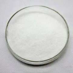
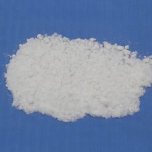
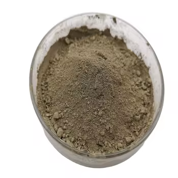
    Zinc stearate, chemically defined as zinc bis(octadecanoate) [Zn(C ₁₇ H ₃₅ COO)], is an organometallic compound identified as a steel soap, developed by the response of stearic acid–; a saturated long-chain fat–; with zinc oxide or zinc salts.

    In its strong type, it works as a hydrophobic lube and release representative, however when refined right into an ultrafine emulsion, its energy increases substantially due to boosted dispersibility and interfacial task.

    The particle features a polar, ionic zinc-containing head group and 2 lengthy hydrophobic alkyl tails, conferring amphiphilic qualities that allow it to function as an internal lubricating substance, water repellent, and surface area modifier in diverse material systems.

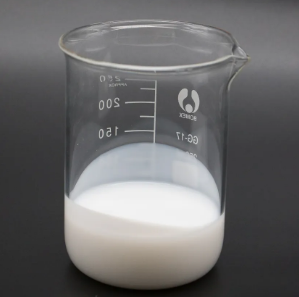
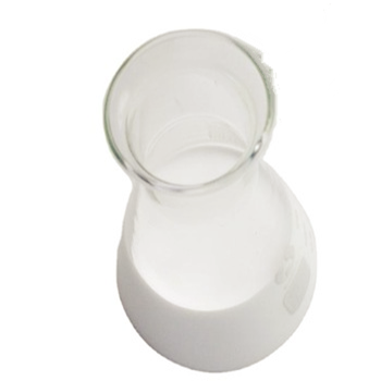
    In liquid solutions, zinc stearate does not dissolve however creates secure colloidal dispersions where submicron particles are stabilized by surfactants or polymeric dispersants versus gathering.

    The “;ultrafine”; designation describes droplet or fragment dimensions commonly listed below 200 nanometers, often in the variety of 50–; 150 nm, which significantly boosts the details area and sensitivity of the spread stage.

    This nanoscale dispersion is critical for achieving uniform distribution in intricate matrices such as polymer thaws, layers, and cementitious systems, where macroscopic agglomerates would certainly jeopardize efficiency.

    1.2 Solution Formation and Stabilization Systems

    The preparation of ultrafine zinc stearate emulsions involves high-energy dispersion strategies such as high-pressure homogenization, ultrasonication, or microfluidization, which break down coarse bits right into nanoscale domain names within an aqueous continual phase.

    To stop coalescence and Ostwald ripening–; processes that destabilize colloids–; nonionic or anionic surfactants (e.g., ethoxylated alcohols, salt dodecyl sulfate) are employed to reduced interfacial tension and supply electrostatic or steric stablizing.

    The selection of emulsifier is critical: it must work with the intended application setting, staying clear of disturbance with downstream processes such as polymer healing or concrete setting.

    In addition, co-emulsifiers or cosolvents may be presented to make improvements the hydrophilic-lipophilic balance (HLB) of the system, ensuring lasting colloidal security under differing pH, temperature, and ionic toughness problems.

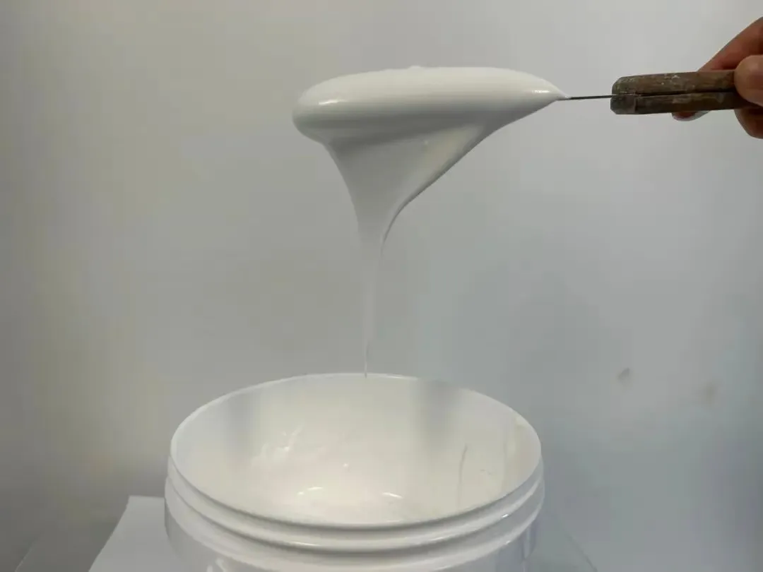
    The resulting emulsion is normally milky white, low-viscosity, and conveniently mixable with water-based formulations, enabling smooth integration right into commercial production lines without customized equipment.


    ( Ultrafine Zinc Stearate Emulsions)

    Correctly created ultrafine solutions can stay steady for months, resisting phase separation, sedimentation, or gelation, which is crucial for consistent efficiency in large-scale production.

    2. Handling Technologies and Bit Size Control

    2.1 High-Energy Dispersion and Nanoemulsification Strategies

    Accomplishing and maintaining ultrafine particle size needs exact control over power input and procedure specifications throughout emulsification.

    High-pressure homogenizers operate at stress surpassing 1000 bar, forcing the pre-emulsion through slim orifices where intense shear, cavitation, and disturbance piece particles right into the nanometer array.

    Ultrasonic processors produce acoustic cavitation in the liquid tool, producing local shock waves that degenerate aggregates and advertise uniform droplet circulation.

    Microfluidization, an extra recent advancement, utilizes fixed-geometry microchannels to develop consistent shear areas, making it possible for reproducible bit size reduction with narrow polydispersity indices (PDI < 0.2).

    These technologies not only lower particle size however additionally boost the crystallinity and surface uniformity of zinc stearate particles, which affects their melting behavior and interaction with host materials.

    Post-processing steps such as purification may be employed to eliminate any kind of residual coarse bits, making certain item uniformity and avoiding problems in delicate applications like thin-film coverings or injection molding.

    2.2 Characterization and Quality Assurance Metrics

    The efficiency of ultrafine zinc stearate emulsions is directly linked to their physical and colloidal buildings, necessitating strenuous analytical characterization.

    Dynamic light scattering (DLS) is regularly used to gauge hydrodynamic diameter and size distribution, while zeta capacity analysis analyzes colloidal stability–; values beyond ± 30 mV generally show good electrostatic stabilization.

    Transmission electron microscopy (TEM) or atomic pressure microscopy (AFM) gives straight visualization of fragment morphology and diffusion quality.

    Thermal evaluation techniques such as differential scanning calorimetry (DSC) determine the melting factor (~ 120–; 130 ° C) and thermal deterioration account, which are crucial for applications entailing high-temperature processing.

    Additionally, security testing under increased problems (elevated temperature, freeze-thaw cycles) guarantees shelf life and robustness during transportation and storage space.

    Suppliers also examine useful efficiency with application-specific tests, such as slip angle dimension for lubricity, water contact angle for hydrophobicity, or diffusion uniformity in polymer composites.

    3. Useful Duties and Efficiency Devices in Industrial Equipment

    3.1 Internal and Exterior Lubrication in Polymer Handling

    In plastics and rubber production, ultrafine zinc stearate emulsions act as very efficient interior and exterior lubricants.

    When incorporated into polymer melts (e.g., PVC, polyolefins, polystyrene), the nanoparticles migrate to interfaces, reducing melt viscosity and friction between polymer chains and handling tools.

    This lowers energy consumption during extrusion and shot molding, reduces die buildup, and enhances surface finish of molded parts.

    Because of their tiny size, ultrafine particles distribute more evenly than powdered zinc stearate, protecting against local lubricant-rich zones that can damage mechanical homes.

    They likewise operate as outside release representatives, creating a thin, non-stick movie on mold and mildew surfaces that helps with part ejection without deposit accumulation.

    This double capability boosts manufacturing effectiveness and item quality in high-speed manufacturing atmospheres.

    3.2 Water Repellency, Anti-Caking, and Surface Area Modification Results

    Past lubrication, these solutions give hydrophobicity to powders, finishings, and building materials.

    When put on cement, pigments, or pharmaceutical powders, the zinc stearate creates a nano-coating that drives away wetness, preventing caking and enhancing flowability during storage and handling.

    In building coverings and renders, incorporation of the emulsion improves water resistance, decreasing water absorption and improving sturdiness versus weathering and freeze-thaw damage.

    The system involves the positioning of stearate particles at interfaces, with hydrophobic tails exposed to the setting, producing a low-energy surface that stands up to wetting.

    Furthermore, in composite products, zinc stearate can change filler-matrix communications, improving dispersion of inorganic fillers like calcium carbonate or talc in polymer matrices.

    This interfacial compatibilization minimizes jumble and improves mechanical efficiency, especially in effect stamina and prolongation at break.

    4. Application Domains and Emerging Technical Frontiers

    4.1 Construction Materials and Cement-Based Equipments

    In the construction market, ultrafine zinc stearate solutions are progressively used as hydrophobic admixtures in concrete, mortar, and plaster.

    They reduce capillary water absorption without endangering compressive strength, therefore improving resistance to chloride ingress, sulfate attack, and carbonation-induced rust of enhancing steel.

    Unlike traditional admixtures that may affect establishing time or air entrainment, zinc stearate solutions are chemically inert in alkaline settings and do not interfere with cement hydration.

    Their nanoscale dispersion guarantees uniform security throughout the matrix, even at reduced dosages (usually 0.5–; 2% by weight of concrete).

    This makes them optimal for infrastructure projects in seaside or high-humidity regions where long-lasting toughness is vital.

    4.2 Advanced Production, Cosmetics, and Nanocomposites

    In innovative manufacturing, these solutions are used in 3D printing powders to improve circulation and decrease moisture level of sensitivity.

    In cosmetics and personal treatment items, they work as appearance modifiers and waterproof agents in foundations, lipsticks, and sunscreens, offering a non-greasy feel and boosted spreadability.

    Emerging applications include their usage in flame-retardant systems, where zinc stearate acts as a synergist by promoting char development in polymer matrices, and in self-cleaning surface areas that combine hydrophobicity with photocatalytic task.

    Research study is also exploring their combination into clever finishes that react to ecological stimulations, such as humidity or mechanical anxiety.

    In summary, ultrafine zinc stearate solutions exhibit how colloidal design transforms a standard additive right into a high-performance useful product.

    By minimizing fragment dimension to the nanoscale and supporting it in aqueous diffusion, these systems attain superior uniformity, sensitivity, and compatibility throughout a broad range of commercial applications.

    As needs for efficiency, resilience, and sustainability grow, ultrafine zinc stearate solutions will continue to play a critical duty in making it possible for next-generation materials and processes.

    5. Distributor

    RBOSCHCO is a trusted global chemical material supplier &; manufacturer with over 12 years experience in providing super high-quality chemicals and Nanomaterials. The company export to many countries, such as USA, Canada, Europe, UAE, South Africa, Tanzania, Kenya, Egypt, Nigeria, Cameroon, Uganda, Turkey, Mexico, Azerbaijan, Belgium, Cyprus, Czech Republic, Brazil, Chile, Argentina, Dubai, Japan, Korea, Vietnam, Thailand, Malaysia, Indonesia, Australia,Germany, France, Italy, Portugal etc. As a leading nanotechnology development manufacturer, RBOSCHCO dominates the market. Our professional work team provides perfect solutions to help improve the efficiency of various industries, create value, and easily cope with various challenges. If you are looking for zinkstearat, please send an email to: [email protected]
    Tags: Ultrafine zinc stearate, zinc stearate, zinc stearate emulsion

    All articles and pictures are from the Internet. If there are any copyright issues, please contact us in time to delete.

    Inquiry us


    • Alumina Ceramic Substrates: The Foundational Enablers of High-Performance Electronic Packaging and Microsystem Integration in Modern Technology alumina al2o3

      Alumina Ceramic Substrates: The Foundational Enablers of High-Performance Electronic Packaging and Microsystem Integration in Modern Technology alumina al2o3

      1. Material Fundamentals and Architectural Qualities of Alumina Ceramics

      1.1 Crystallographic and Compositional Basis of α-Alumina


      (Alumina Ceramic Substrates)

      Alumina ceramic substratums, mostly made up of light weight aluminum oxide (Al ₂ O ₃), act as the backbone of modern electronic product packaging because of their phenomenal equilibrium of electrical insulation, thermal stability, mechanical strength, and manufacturability.

      The most thermodynamically steady phase of alumina at heats is corundum, or α-Al Two O TWO, which crystallizes in a hexagonal close-packed oxygen latticework with aluminum ions occupying two-thirds of the octahedral interstitial websites.

      This thick atomic plan imparts high hardness (Mohs 9), superb wear resistance, and solid chemical inertness, making α-alumina appropriate for rough operating environments.

      Commercial substratums usually contain 90–; 99.8% Al ₂ O FOUR, with minor additions of silica (SiO TWO), magnesia (MgO), or uncommon earth oxides used as sintering aids to advertise densification and control grain development during high-temperature handling.

      Greater pureness qualities (e.g., 99.5% and over) display remarkable electrical resistivity and thermal conductivity, while lower pureness variations (90; 96%) offer affordable solutions for less demanding applications.

      1.2 Microstructure and Defect Design for Electronic Reliability

      The efficiency of alumina substrates in digital systems is seriously based on microstructural harmony and issue reduction.

      A fine, equiaxed grain structure–; usually ranging from 1 to 10 micrometers–; makes certain mechanical stability and lowers the probability of crack breeding under thermal or mechanical anxiety.

      Porosity, especially interconnected or surface-connected pores, must be minimized as it degrades both mechanical toughness and dielectric performance.

      Advanced processing strategies such as tape spreading, isostatic pressing, and regulated sintering in air or managed environments enable the production of substrates with near-theoretical thickness (> 99.5%) and surface area roughness below 0.5 µm, crucial for thin-film metallization and cable bonding.

      Additionally, impurity segregation at grain borders can result in leak currents or electrochemical migration under prejudice, requiring rigorous control over raw material purity and sintering problems to make certain long-lasting integrity in moist or high-voltage environments.

      2. Production Processes and Substratum Construction Technologies


      ( Alumina Ceramic Substrates)

      2.1 Tape Spreading and Eco-friendly Body Processing

      The manufacturing of alumina ceramic substrates begins with the prep work of an extremely dispersed slurry containing submicron Al ₂ O three powder, organic binders, plasticizers, dispersants, and solvents.

      This slurry is processed by means of tape spreading–; a continuous method where the suspension is topped a relocating carrier film utilizing a precision medical professional blade to achieve uniform thickness, typically between 0.1 mm and 1.0 mm.

      After solvent dissipation, the resulting “;eco-friendly tape”; is flexible and can be punched, drilled, or laser-cut to form through openings for upright interconnections.

      Multiple layers may be laminated to produce multilayer substrates for intricate circuit assimilation, although the majority of commercial applications use single-layer configurations due to set you back and thermal development considerations.

      The environment-friendly tapes are then meticulously debound to eliminate organic additives with regulated thermal disintegration before last sintering.

      2.2 Sintering and Metallization for Circuit Combination

      Sintering is performed in air at temperatures in between 1550 ° C and 1650 ° C, where solid-state diffusion drives pore elimination and grain coarsening to achieve full densification.

      The direct shrinkage throughout sintering–; typically 15–; 20%; need to be precisely forecasted and made up for in the style of environment-friendly tapes to make certain dimensional precision of the final substratum.

      Complying with sintering, metallization is put on create conductive traces, pads, and vias.

      2 key techniques dominate: thick-film printing and thin-film deposition.

      In thick-film innovation, pastes having steel powders (e.g., tungsten, molybdenum, or silver-palladium alloys) are screen-printed onto the substratum and co-fired in a reducing ambience to develop durable, high-adhesion conductors.

      For high-density or high-frequency applications, thin-film procedures such as sputtering or dissipation are utilized to down payment bond layers (e.g., titanium or chromium) complied with by copper or gold, enabling sub-micron pattern by means of photolithography.

      Vias are full of conductive pastes and fired to develop electric interconnections between layers in multilayer styles.

      3. Functional Qualities and Efficiency Metrics in Electronic Equipment

      3.1 Thermal and Electric Habits Under Functional Tension

      Alumina substrates are valued for their beneficial combination of moderate thermal conductivity (20; 35 W/m · K for 96–; 99.8% Al ₂ O THREE), which makes it possible for reliable warm dissipation from power tools, and high quantity resistivity (> 10 ¹⁴ Ω · centimeters), ensuring marginal leak current.

      Their dielectric constant (εᵣ ≈ 9–; 10 at 1 MHz) is secure over a wide temperature and regularity variety, making them appropriate for high-frequency circuits up to numerous ghzs, although lower-κ materials like light weight aluminum nitride are chosen for mm-wave applications.

      The coefficient of thermal development (CTE) of alumina (~ 6.8–; 7.2 ppm/K) is fairly well-matched to that of silicon (~ 3 ppm/K) and certain packaging alloys, lowering thermo-mechanical tension during gadget operation and thermal cycling.

      However, the CTE mismatch with silicon stays a problem in flip-chip and straight die-attach setups, typically calling for compliant interposers or underfill products to minimize fatigue failing.

      3.2 Mechanical Effectiveness and Environmental Durability

      Mechanically, alumina substratums show high flexural strength (300; 400 MPa) and excellent dimensional stability under lots, allowing their usage in ruggedized electronics for aerospace, automobile, and commercial control systems.

      They are immune to vibration, shock, and creep at raised temperatures, maintaining structural stability as much as 1500 ° C in inert ambiences.

      In moist atmospheres, high-purity alumina reveals minimal wetness absorption and outstanding resistance to ion movement, making certain long-term integrity in outside and high-humidity applications.

      Surface firmness likewise secures versus mechanical damages during handling and assembly, although treatment should be taken to prevent edge chipping due to fundamental brittleness.

      4. Industrial Applications and Technological Influence Across Sectors

      4.1 Power Electronics, RF Modules, and Automotive Equipments

      Alumina ceramic substrates are ubiquitous in power electronic modules, consisting of insulated gate bipolar transistors (IGBTs), MOSFETs, and rectifiers, where they provide electric isolation while promoting heat transfer to warmth sinks.

      In radio frequency (RF) and microwave circuits, they function as service provider systems for hybrid integrated circuits (HICs), surface area acoustic wave (SAW) filters, and antenna feed networks due to their secure dielectric homes and reduced loss tangent.

      In the auto market, alumina substratums are utilized in engine control devices (ECUs), sensor plans, and electric lorry (EV) power converters, where they withstand heats, thermal biking, and direct exposure to destructive liquids.

      Their dependability under severe problems makes them important for safety-critical systems such as anti-lock braking (ABDOMINAL MUSCLE) and progressed driver help systems (ADAS).

      4.2 Medical Instruments, Aerospace, and Arising Micro-Electro-Mechanical Solutions

      Beyond customer and industrial electronics, alumina substratums are utilized in implantable clinical devices such as pacemakers and neurostimulators, where hermetic sealing and biocompatibility are vital.

      In aerospace and defense, they are made use of in avionics, radar systems, and satellite interaction modules as a result of their radiation resistance and stability in vacuum cleaner settings.

      Furthermore, alumina is increasingly used as a structural and protecting system in micro-electro-mechanical systems (MEMS), consisting of pressure sensors, accelerometers, and microfluidic tools, where its chemical inertness and compatibility with thin-film handling are beneficial.

      As digital systems remain to require greater power thickness, miniaturization, and integrity under severe conditions, alumina ceramic substratums continue to be a keystone product, linking the space in between efficiency, expense, and manufacturability in innovative digital product packaging.

      5. Supplier

      Alumina Technology Co., Ltd focus on the research and development, production and sales of aluminum oxide powder, aluminum oxide products, aluminum oxide crucible, etc., serving the electronics, ceramics, chemical and other industries. Since its establishment in 2005, the company has been committed to providing customers with the best products and services. If you are looking for high quality alumina al2o3, please feel free to contact us. ([email protected])
      Tags: Alumina Ceramic Substrates, Alumina Ceramics, alumina

      All articles and pictures are from the Internet. If there are any copyright issues, please contact us in time to delete.

      Inquiry us


      • Transparent Ceramics: Engineering Light Transmission in Polycrystalline Inorganic Solids for Next-Generation Photonic and Structural Applications alumina bricks

        Transparent Ceramics: Engineering Light Transmission in Polycrystalline Inorganic Solids for Next-Generation Photonic and Structural Applications alumina bricks

        1. Essential Composition and Structural Architecture of Quartz Ceramics

        1.1 Crystalline vs. Fused Silica: Defining the Product Class


        (Transparent Ceramics)

        Quartz porcelains, likewise known as merged quartz or fused silica ceramics, are innovative inorganic materials stemmed from high-purity crystalline quartz (SiO TWO) that go through regulated melting and loan consolidation to develop a dense, non-crystalline (amorphous) or partly crystalline ceramic framework.

        Unlike traditional porcelains such as alumina or zirconia, which are polycrystalline and made up of multiple stages, quartz ceramics are mainly composed of silicon dioxide in a network of tetrahedrally coordinated SiO four systems, supplying outstanding chemical purity–; frequently exceeding 99.9% SiO ₂.

        The difference between integrated quartz and quartz porcelains hinges on processing: while fused quartz is typically a completely amorphous glass developed by fast cooling of liquified silica, quartz porcelains may involve regulated crystallization (devitrification) or sintering of fine quartz powders to accomplish a fine-grained polycrystalline or glass-ceramic microstructure with boosted mechanical robustness.

        This hybrid method combines the thermal and chemical stability of fused silica with boosted crack sturdiness and dimensional security under mechanical load.

        1.2 Thermal and Chemical Stability Mechanisms

        The exceptional performance of quartz porcelains in extreme environments comes from the strong covalent Si–; O bonds that create a three-dimensional network with high bond energy (~ 452 kJ/mol), conferring amazing resistance to thermal deterioration and chemical strike.

        These products exhibit an exceptionally reduced coefficient of thermal expansion–; about 0.55 × 10 ⁻⁶/ K over the range 20–; 300 ° C–; making them very resistant to thermal shock, a critical characteristic in applications involving rapid temperature cycling.

        They keep architectural integrity from cryogenic temperature levels up to 1200 ° C in air, and also greater in inert environments, before softening begins around 1600 ° C.

        Quartz ceramics are inert to most acids, including hydrochloric, nitric, and sulfuric acids, due to the security of the SiO two network, although they are at risk to assault by hydrofluoric acid and solid alkalis at raised temperature levels.

        This chemical resilience, combined with high electrical resistivity and ultraviolet (UV) openness, makes them excellent for usage in semiconductor processing, high-temperature furnaces, and optical systems exposed to extreme conditions.

        2. Production Processes and Microstructural Control


        ( Transparent Ceramics)

        2.1 Melting, Sintering, and Devitrification Pathways

        The manufacturing of quartz ceramics entails advanced thermal handling techniques developed to protect purity while accomplishing wanted thickness and microstructure.

        One common approach is electrical arc melting of high-purity quartz sand, followed by controlled cooling to create integrated quartz ingots, which can after that be machined into elements.

        For sintered quartz ceramics, submicron quartz powders are compacted via isostatic pushing and sintered at temperature levels between 1100 ° C and 1400 ° C, commonly with marginal ingredients to promote densification without inducing too much grain development or stage change.

        An essential obstacle in processing is staying clear of devitrification–; the spontaneous condensation of metastable silica glass right into cristobalite or tridymite stages–; which can endanger thermal shock resistance due to volume modifications during stage changes.

        Producers employ specific temperature level control, quick air conditioning cycles, and dopants such as boron or titanium to subdue unwanted condensation and preserve a secure amorphous or fine-grained microstructure.

        2.2 Additive Production and Near-Net-Shape Fabrication

        Recent developments in ceramic additive production (AM), particularly stereolithography (SHANTY TOWN) and binder jetting, have actually allowed the construction of intricate quartz ceramic parts with high geometric accuracy.

        In these procedures, silica nanoparticles are put on hold in a photosensitive material or selectively bound layer-by-layer, complied with by debinding and high-temperature sintering to achieve complete densification.

        This approach minimizes product waste and permits the creation of complex geometries–; such as fluidic channels, optical cavities, or warm exchanger components–; that are challenging or difficult to attain with standard machining.

        Post-processing techniques, consisting of chemical vapor infiltration (CVI) or sol-gel finishing, are occasionally put on secure surface porosity and improve mechanical and ecological toughness.

        These advancements are increasing the application extent of quartz ceramics right into micro-electromechanical systems (MEMS), lab-on-a-chip tools, and customized high-temperature fixtures.

        3. Useful Characteristics and Efficiency in Extreme Environments

        3.1 Optical Transparency and Dielectric Habits

        Quartz ceramics exhibit special optical homes, including high transmission in the ultraviolet, noticeable, and near-infrared spectrum (from ~ 180 nm to 2500 nm), making them crucial in UV lithography, laser systems, and space-based optics.

        This openness occurs from the absence of electronic bandgap transitions in the UV-visible array and very little scattering as a result of homogeneity and low porosity.

        In addition, they have superb dielectric buildings, with a low dielectric constant (~ 3.8 at 1 MHz) and very little dielectric loss, allowing their use as shielding elements in high-frequency and high-power digital systems, such as radar waveguides and plasma reactors.

        Their capability to maintain electrical insulation at elevated temperature levels better boosts integrity sought after electrical environments.

        3.2 Mechanical Actions and Long-Term Durability

        In spite of their high brittleness–; a common quality among porcelains–; quartz porcelains demonstrate excellent mechanical toughness (flexural stamina up to 100 MPa) and exceptional creep resistance at high temperatures.

        Their firmness (around 5.5–; 6.5 on the Mohs scale) gives resistance to surface area abrasion, although treatment has to be taken throughout dealing with to prevent damaging or split proliferation from surface problems.

        Ecological toughness is an additional vital advantage: quartz porcelains do not outgas dramatically in vacuum cleaner, resist radiation damage, and preserve dimensional security over prolonged exposure to thermal cycling and chemical settings.

        This makes them favored products in semiconductor fabrication chambers, aerospace sensors, and nuclear instrumentation where contamination and failing must be decreased.

        4. Industrial, Scientific, and Arising Technical Applications

        4.1 Semiconductor and Photovoltaic Manufacturing Solutions

        In the semiconductor industry, quartz porcelains are ubiquitous in wafer handling tools, including heating system tubes, bell jars, susceptors, and shower heads made use of in chemical vapor deposition (CVD) and plasma etching.

        Their purity protects against metal contamination of silicon wafers, while their thermal security makes certain uniform temperature distribution throughout high-temperature processing actions.

        In photovoltaic or pv manufacturing, quartz components are used in diffusion heaters and annealing systems for solar battery production, where constant thermal accounts and chemical inertness are essential for high return and effectiveness.

        The need for bigger wafers and higher throughput has actually driven the development of ultra-large quartz ceramic structures with boosted homogeneity and minimized flaw thickness.

        4.2 Aerospace, Defense, and Quantum Modern Technology Assimilation

        Beyond industrial handling, quartz porcelains are utilized in aerospace applications such as rocket support windows, infrared domes, and re-entry automobile parts as a result of their capacity to stand up to extreme thermal gradients and aerodynamic tension.

        In protection systems, their openness to radar and microwave frequencies makes them appropriate for radomes and sensor housings.

        More recently, quartz ceramics have actually located duties in quantum innovations, where ultra-low thermal expansion and high vacuum cleaner compatibility are needed for precision optical dental caries, atomic catches, and superconducting qubit rooms.

        Their ability to minimize thermal drift makes sure lengthy comprehensibility times and high measurement accuracy in quantum computer and sensing systems.

        In recap, quartz porcelains represent a course of high-performance products that connect the void in between standard porcelains and specialized glasses.

        Their unparalleled mix of thermal stability, chemical inertness, optical transparency, and electric insulation allows modern technologies operating at the limits of temperature level, purity, and precision.

        As manufacturing techniques evolve and require grows for materials with the ability of standing up to increasingly extreme conditions, quartz ceramics will remain to play a foundational function ahead of time semiconductor, awood, aerospace, and quantum systems.

        5. Supplier

        Advanced Ceramics founded on October 17, 2012, is a high-tech enterprise committed to the research and development, production, processing, sales and technical services of ceramic relative materials and products. Our products includes but not limited to Boron Carbide Ceramic Products, Boron Nitride Ceramic Products, Silicon Carbide Ceramic Products, Silicon Nitride Ceramic Products, Zirconium Dioxide Ceramic Products, etc. If you are interested, please feel free to contact us.([email protected])
        Tags: Transparent Ceramics, ceramic dish, ceramic piping

        All articles and pictures are from the Internet. If there are any copyright issues, please contact us in time to delete.

        Inquiry us


        • Lightweight Concrete Foam Generators: Engineering Precision in Cellular Concrete Fabrication for Sustainable Construction potassium silicate powder

          Lightweight Concrete Foam Generators: Engineering Precision in Cellular Concrete Fabrication for Sustainable Construction potassium silicate powder

          1. Molecular Design and Physicochemical Foundations of Potassium Silicate

          1.1 Chemical Make-up and Polymerization Habits in Aqueous Solutions


          (Potassium Silicate)

          Potassium silicate (K TWO O · nSiO ₂), frequently referred to as water glass or soluble glass, is a not natural polymer developed by the blend of potassium oxide (K TWO O) and silicon dioxide (SiO TWO) at raised temperature levels, followed by dissolution in water to generate a thick, alkaline solution.

          Unlike sodium silicate, its even more usual equivalent, potassium silicate uses exceptional sturdiness, enhanced water resistance, and a reduced propensity to effloresce, making it especially valuable in high-performance layers and specialty applications.

          The ratio of SiO ₂ to K ₂ O, denoted as “;n”; (modulus), regulates the material’;s residential properties: low-modulus solutions (n < 2.5) are highly soluble and responsive, while high-modulus systems (n > 3.0) show better water resistance and film-forming ability yet reduced solubility.

          In liquid atmospheres, potassium silicate goes through dynamic condensation reactions, where silanol (Si–; OH) groups polymerize to develop siloxane (Si–; O–; Si) networks–; a procedure analogous to natural mineralization.

          This vibrant polymerization enables the development of three-dimensional silica gels upon drying or acidification, developing dense, chemically immune matrices that bond highly with substrates such as concrete, steel, and ceramics.

          The high pH of potassium silicate options (usually 10–; 13) helps with quick reaction with climatic CO ₂ or surface hydroxyl teams, increasing the development of insoluble silica-rich layers.

          1.2 Thermal Security and Structural Change Under Extreme Conditions

          One of the specifying qualities of potassium silicate is its phenomenal thermal stability, allowing it to endure temperature levels surpassing 1000 ° C without significant disintegration.

          When exposed to heat, the moisturized silicate network dries out and densifies, eventually transforming into a glassy, amorphous potassium silicate ceramic with high mechanical toughness and thermal shock resistance.

          This actions underpins its use in refractory binders, fireproofing layers, and high-temperature adhesives where organic polymers would break down or combust.

          The potassium cation, while much more unpredictable than sodium at extreme temperature levels, adds to decrease melting factors and improved sintering habits, which can be beneficial in ceramic handling and glaze formulations.

          In addition, the capacity of potassium silicate to react with steel oxides at raised temperature levels allows the formation of complicated aluminosilicate or alkali silicate glasses, which are integral to sophisticated ceramic composites and geopolymer systems.


          ( Potassium Silicate)

          2. Industrial and Building Applications in Sustainable Infrastructure

          2.1 Function in Concrete Densification and Surface Setting

          In the construction market, potassium silicate has gotten importance as a chemical hardener and densifier for concrete surface areas, dramatically boosting abrasion resistance, dust control, and long-term durability.

          Upon application, the silicate types permeate the concrete’;s capillary pores and react with complimentary calcium hydroxide (Ca(OH)); a result of cement hydration–; to form calcium silicate hydrate (C-S-H), the same binding stage that offers concrete its stamina.

          This pozzolanic response properly “;seals”; the matrix from within, lowering permeability and hindering the ingress of water, chlorides, and various other destructive agents that result in reinforcement rust and spalling.

          Contrasted to traditional sodium-based silicates, potassium silicate produces less efflorescence because of the greater solubility and mobility of potassium ions, causing a cleaner, extra aesthetically pleasing finish–; especially essential in building concrete and refined flooring systems.

          Additionally, the boosted surface hardness improves resistance to foot and car traffic, prolonging life span and lowering maintenance prices in industrial facilities, stockrooms, and auto parking structures.

          2.2 Fireproof Coatings and Passive Fire Protection Systems

          Potassium silicate is an essential component in intumescent and non-intumescent fireproofing coatings for structural steel and other combustible substratums.

          When exposed to heats, the silicate matrix undergoes dehydration and increases in conjunction with blowing representatives and char-forming resins, producing a low-density, insulating ceramic layer that guards the hidden material from heat.

          This protective barrier can maintain architectural integrity for as much as several hours during a fire event, offering important time for discharge and firefighting operations.

          The not natural nature of potassium silicate makes certain that the coating does not create hazardous fumes or contribute to flame spread, meeting rigid environmental and security laws in public and business buildings.

          Furthermore, its excellent bond to metal substrates and resistance to maturing under ambient conditions make it excellent for lasting passive fire protection in overseas platforms, tunnels, and high-rise constructions.

          3. Agricultural and Environmental Applications for Sustainable Advancement

          3.1 Silica Shipment and Plant Wellness Enhancement in Modern Agriculture

          In agronomy, potassium silicate acts as a dual-purpose amendment, supplying both bioavailable silica and potassium–; 2 necessary elements for plant development and stress resistance.

          Silica is not identified as a nutrient however plays a crucial structural and defensive role in plants, gathering in cell walls to form a physical barrier against insects, pathogens, and ecological stressors such as drought, salinity, and heavy steel poisoning.

          When used as a foliar spray or soil soak, potassium silicate dissociates to launch silicic acid (Si(OH)), which is absorbed by plant roots and delivered to cells where it polymerizes right into amorphous silica down payments.

          This support improves mechanical stamina, lowers lodging in grains, and boosts resistance to fungal infections like powdery mold and blast disease.

          All at once, the potassium component sustains crucial physiological processes consisting of enzyme activation, stomatal law, and osmotic equilibrium, contributing to improved return and plant top quality.

          Its use is particularly helpful in hydroponic systems and silica-deficient soils, where traditional sources like rice husk ash are impractical.

          3.2 Soil Stabilization and Disintegration Control in Ecological Engineering

          Beyond plant nutrition, potassium silicate is employed in dirt stablizing modern technologies to alleviate disintegration and enhance geotechnical buildings.

          When injected right into sandy or loosened dirts, the silicate service penetrates pore areas and gels upon direct exposure to carbon monoxide two or pH changes, binding soil fragments right into a natural, semi-rigid matrix.

          This in-situ solidification method is made use of in slope stabilization, foundation reinforcement, and land fill capping, supplying an ecologically benign choice to cement-based cements.

          The resulting silicate-bonded dirt shows improved shear stamina, minimized hydraulic conductivity, and resistance to water disintegration, while staying permeable enough to allow gas exchange and origin infiltration.

          In ecological repair projects, this method supports plants facility on degraded lands, advertising long-term community recovery without presenting synthetic polymers or relentless chemicals.

          4. Arising Duties in Advanced Products and Environment-friendly Chemistry

          4.1 Precursor for Geopolymers and Low-Carbon Cementitious Solutions

          As the building market seeks to lower its carbon impact, potassium silicate has actually emerged as an important activator in alkali-activated materials and geopolymers–; cement-free binders derived from industrial results such as fly ash, slag, and metakaolin.

          In these systems, potassium silicate offers the alkaline environment and soluble silicate species needed to dissolve aluminosilicate forerunners and re-polymerize them into a three-dimensional aluminosilicate connect with mechanical residential or commercial properties equaling average Portland cement.

          Geopolymers turned on with potassium silicate show exceptional thermal security, acid resistance, and decreased contraction compared to sodium-based systems, making them ideal for severe settings and high-performance applications.

          In addition, the manufacturing of geopolymers creates up to 80% less carbon monoxide ₂ than conventional cement, positioning potassium silicate as a key enabler of lasting building and construction in the era of environment adjustment.

          4.2 Useful Additive in Coatings, Adhesives, and Flame-Retardant Textiles

          Beyond architectural materials, potassium silicate is locating new applications in useful finishes and clever materials.

          Its ability to develop hard, transparent, and UV-resistant movies makes it suitable for safety coverings on rock, masonry, and historical monuments, where breathability and chemical compatibility are essential.

          In adhesives, it serves as a not natural crosslinker, improving thermal security and fire resistance in laminated timber products and ceramic assemblies.

          Current study has additionally explored its usage in flame-retardant textile therapies, where it creates a safety lustrous layer upon exposure to flame, avoiding ignition and melt-dripping in synthetic textiles.

          These technologies emphasize the versatility of potassium silicate as an eco-friendly, non-toxic, and multifunctional product at the junction of chemistry, design, and sustainability.

          5. Distributor

          Cabr-Concrete is a supplier of Concrete Admixture with over 12 years of experience in nano-building energy conservation and nanotechnology development. It accepts payment via Credit Card, T/T, West Union and Paypal. TRUNNANO will ship the goods to customers overseas through FedEx, DHL, by air, or by sea. If you are looking for high quality Concrete Admixture, please feel free to contact us and send an inquiry.
          Tags: potassium silicate,k silicate,potassium silicate fertilizer

          All articles and pictures are from the Internet. If there are any copyright issues, please contact us in time to delete.

          Inquiry us


          • Chromium(III) Oxide (Cr₂O₃): From Inert Pigment to Functional Material in Catalysis, Electronics, and Surface Engineering chrome oxide

            Chromium(III) Oxide (Cr₂O₃): From Inert Pigment to Functional Material in Catalysis, Electronics, and Surface Engineering chrome oxide

            1. Basic Chemistry and Structural Quality of Chromium(III) Oxide

            1.1 Crystallographic Framework and Electronic Setup


            (Chromium Oxide)

            Chromium(III) oxide, chemically denoted as Cr two O FOUR, is a thermodynamically steady inorganic compound that belongs to the family of shift steel oxides exhibiting both ionic and covalent attributes.

            It crystallizes in the diamond structure, a rhombohedral lattice (room group R-3c), where each chromium ion is octahedrally worked with by six oxygen atoms, and each oxygen is surrounded by four chromium atoms in a close-packed arrangement.

            This architectural concept, shared with α-Fe two O THREE (hematite) and Al Two O ₃ (corundum), passes on phenomenal mechanical hardness, thermal security, and chemical resistance to Cr ₂ O SIX.

            The digital configuration of Cr FOUR ⁺ is [Ar] 3d ³, and in the octahedral crystal area of the oxide latticework, the 3 d-electrons occupy the lower-energy t ₂ g orbitals, resulting in a high-spin state with considerable exchange communications.

            These interactions generate antiferromagnetic ordering listed below the Néel temperature of around 307 K, although weak ferromagnetism can be observed due to rotate canting in particular nanostructured types.

            The broad bandgap of Cr ₂ O FOUR–; ranging from 3.0 to 3.5 eV–; makes it an electrical insulator with high resistivity, making it transparent to visible light in thin-film kind while showing up dark environment-friendly in bulk as a result of solid absorption in the red and blue regions of the range.

            1.2 Thermodynamic Security and Surface Sensitivity

            Cr ₂ O ₃ is just one of one of the most chemically inert oxides understood, displaying remarkable resistance to acids, alkalis, and high-temperature oxidation.

            This security arises from the solid Cr–; O bonds and the low solubility of the oxide in liquid settings, which likewise contributes to its ecological perseverance and reduced bioavailability.

            However, under extreme problems–; such as concentrated warm sulfuric or hydrofluoric acid–; Cr ₂ O six can gradually liquify, forming chromium salts.

            The surface of Cr ₂ O five is amphoteric, with the ability of interacting with both acidic and standard types, which enables its usage as a stimulant support or in ion-exchange applications.


            ( Chromium Oxide)

            Surface hydroxyl groups (; OH) can form with hydration, affecting its adsorption actions towards steel ions, organic molecules, and gases.

            In nanocrystalline or thin-film types, the increased surface-to-volume ratio enhances surface area sensitivity, allowing for functionalization or doping to tailor its catalytic or digital properties.

            2. Synthesis and Handling Methods for Practical Applications

            2.1 Traditional and Advanced Manufacture Routes

            The production of Cr two O three extends a range of methods, from industrial-scale calcination to accuracy thin-film deposition.

            The most usual commercial course involves the thermal decay of ammonium dichromate ((NH ₄)₂ Cr Two O ₇) or chromium trioxide (CrO SIX) at temperature levels over 300 ° C, generating high-purity Cr ₂ O two powder with regulated fragment dimension.

            Additionally, the decrease of chromite ores (FeCr two O FOUR) in alkaline oxidative settings produces metallurgical-grade Cr ₂ O three made use of in refractories and pigments.

            For high-performance applications, progressed synthesis strategies such as sol-gel handling, burning synthesis, and hydrothermal approaches enable fine control over morphology, crystallinity, and porosity.

            These techniques are especially useful for creating nanostructured Cr ₂ O five with enhanced surface for catalysis or sensing unit applications.

            2.2 Thin-Film Deposition and Epitaxial Growth

            In electronic and optoelectronic contexts, Cr two O two is frequently transferred as a slim film making use of physical vapor deposition (PVD) techniques such as sputtering or electron-beam evaporation.

            Chemical vapor deposition (CVD) and atomic layer deposition (ALD) offer superior conformality and density control, crucial for integrating Cr ₂ O ₃ into microelectronic tools.

            Epitaxial growth of Cr two O six on lattice-matched substrates like α-Al two O three or MgO enables the formation of single-crystal films with minimal issues, making it possible for the research of intrinsic magnetic and digital buildings.

            These top quality films are critical for arising applications in spintronics and memristive gadgets, where interfacial top quality straight influences gadget performance.

            3. Industrial and Environmental Applications of Chromium Oxide

            3.1 Duty as a Resilient Pigment and Abrasive Product

            One of the oldest and most prevalent uses of Cr ₂ O Six is as an eco-friendly pigment, historically known as “;chrome environment-friendly”; or “;viridian”; in imaginative and industrial finishes.

            Its extreme color, UV stability, and resistance to fading make it perfect for building paints, ceramic glazes, tinted concretes, and polymer colorants.

            Unlike some natural pigments, Cr two O six does not deteriorate under extended sunlight or heats, ensuring long-lasting aesthetic toughness.

            In rough applications, Cr two O three is utilized in polishing substances for glass, steels, and optical elements as a result of its hardness (Mohs hardness of ~ 8–; 8.5) and fine particle dimension.

            It is specifically reliable in precision lapping and completing procedures where marginal surface damage is needed.

            3.2 Use in Refractories and High-Temperature Coatings

            Cr ₂ O two is a crucial component in refractory materials used in steelmaking, glass manufacturing, and concrete kilns, where it supplies resistance to thaw slags, thermal shock, and destructive gases.

            Its high melting factor (~ 2435 ° C) and chemical inertness enable it to keep structural integrity in severe atmospheres.

            When combined with Al ₂ O two to form chromia-alumina refractories, the product exhibits enhanced mechanical toughness and deterioration resistance.

            In addition, plasma-sprayed Cr two O five finishings are applied to turbine blades, pump seals, and shutoffs to boost wear resistance and lengthen life span in hostile commercial setups.

            4. Emerging Roles in Catalysis, Spintronics, and Memristive Tools

            4.1 Catalytic Task in Dehydrogenation and Environmental Remediation

            Although Cr Two O three is usually taken into consideration chemically inert, it exhibits catalytic activity in details reactions, particularly in alkane dehydrogenation procedures.

            Industrial dehydrogenation of lp to propylene–; a vital step in polypropylene production–; frequently uses Cr two O four sustained on alumina (Cr/Al two O FOUR) as the active driver.

            In this context, Cr TWO ⁺ sites help with C–; H bond activation, while the oxide matrix maintains the dispersed chromium species and protects against over-oxidation.

            The catalyst’;s performance is highly sensitive to chromium loading, calcination temperature, and reduction conditions, which affect the oxidation state and coordination setting of energetic websites.

            Past petrochemicals, Cr two O ₃-based materials are discovered for photocatalytic deterioration of natural toxins and carbon monoxide oxidation, specifically when doped with transition steels or paired with semiconductors to improve cost splitting up.

            4.2 Applications in Spintronics and Resistive Changing Memory

            Cr Two O six has actually gotten attention in next-generation digital tools because of its distinct magnetic and electric residential properties.

            It is a paradigmatic antiferromagnetic insulator with a linear magnetoelectric result, indicating its magnetic order can be controlled by an electrical field and vice versa.

            This property enables the development of antiferromagnetic spintronic tools that are unsusceptible to exterior electromagnetic fields and run at high speeds with low power usage.

            Cr Two O FOUR-based passage junctions and exchange prejudice systems are being investigated for non-volatile memory and logic gadgets.

            Additionally, Cr two O five exhibits memristive behavior–; resistance changing generated by electric fields–; making it a prospect for resisting random-access memory (ReRAM).

            The changing mechanism is attributed to oxygen vacancy migration and interfacial redox procedures, which modulate the conductivity of the oxide layer.

            These capabilities placement Cr two O ₃ at the forefront of study into beyond-silicon computer architectures.

            In summary, chromium(III) oxide transcends its typical role as an easy pigment or refractory additive, emerging as a multifunctional product in innovative technical domain names.

            Its combination of architectural toughness, electronic tunability, and interfacial activity makes it possible for applications varying from industrial catalysis to quantum-inspired electronic devices.

            As synthesis and characterization techniques development, Cr two O two is positioned to play an increasingly crucial function in sustainable production, energy conversion, and next-generation infotech.

            5. Provider

            TRUNNANO is a supplier of Spherical Tungsten Powder with over 12 years of experience in nano-building energy conservation and nanotechnology development. It accepts payment via Credit Card, T/T, West Union and Paypal. Trunnano will ship the goods to customers overseas through FedEx, DHL, by air, or by sea. If you want to know more about Spherical Tungsten Powder, please feel free to contact us and send an inquiry([email protected]).
            Tags: Chromium Oxide, Cr₂O₃, High-Purity Chromium Oxide

            All articles and pictures are from the Internet. If there are any copyright issues, please contact us in time to delete.

            Inquiry us


            • Silicon Carbide (SiC): The Wide-Bandgap Semiconductor Revolutionizing Power Electronics and Extreme-Environment Technologies sic compound

              Silicon Carbide (SiC): The Wide-Bandgap Semiconductor Revolutionizing Power Electronics and Extreme-Environment Technologies sic compound

              1. Basic Features and Crystallographic Variety of Silicon Carbide

              1.1 Atomic Structure and Polytypic Intricacy


              (Silicon Carbide Powder)

              Silicon carbide (SiC) is a binary substance made up of silicon and carbon atoms set up in an extremely steady covalent latticework, identified by its extraordinary hardness, thermal conductivity, and digital residential properties.

              Unlike conventional semiconductors such as silicon or germanium, SiC does not exist in a single crystal structure however manifests in over 250 distinctive polytypes–; crystalline types that differ in the piling sequence of silicon-carbon bilayers along the c-axis.

              The most highly relevant polytypes consist of 3C-SiC (cubic, zincblende framework), 4H-SiC, and 6H-SiC (both hexagonal), each showing subtly various digital and thermal attributes.

              Among these, 4H-SiC is especially preferred for high-power and high-frequency digital gadgets as a result of its higher electron flexibility and lower on-resistance contrasted to various other polytypes.

              The strong covalent bonding–; comprising about 88% covalent and 12% ionic personality–; provides remarkable mechanical toughness, chemical inertness, and resistance to radiation damages, making SiC appropriate for procedure in extreme environments.

              1.2 Electronic and Thermal Attributes

              The electronic supremacy of SiC stems from its wide bandgap, which ranges from 2.3 eV (3C-SiC) to 3.3 eV (4H-SiC), dramatically bigger than silicon’;s 1.1 eV.

              This large bandgap makes it possible for SiC gadgets to operate at much higher temperature levels–; as much as 600 ° C–; without intrinsic provider generation overwhelming the device, a vital constraint in silicon-based electronic devices.

              Furthermore, SiC possesses a high important electrical field strength (~ 3 MV/cm), approximately ten times that of silicon, enabling thinner drift layers and higher break down voltages in power devices.

              Its thermal conductivity (~ 3.7–; 4.9 W/cm · K for 4H-SiC) surpasses that of copper, assisting in efficient warmth dissipation and lowering the requirement for intricate cooling systems in high-power applications.

              Incorporated with a high saturation electron speed (~ 2 × 10 ⁷ cm/s), these buildings make it possible for SiC-based transistors and diodes to change quicker, deal with higher voltages, and operate with better energy performance than their silicon counterparts.

              These qualities jointly place SiC as a foundational material for next-generation power electronics, especially in electric automobiles, renewable energy systems, and aerospace technologies.


              ( Silicon Carbide Powder)

              2. Synthesis and Construction of High-Quality Silicon Carbide Crystals

              2.1 Mass Crystal Development through Physical Vapor Transportation

              The production of high-purity, single-crystal SiC is among the most difficult aspects of its technical deployment, mostly because of its high sublimation temperature (~ 2700 ° C )and complex polytype control.

              The leading technique for bulk growth is the physical vapor transportation (PVT) strategy, additionally referred to as the modified Lely method, in which high-purity SiC powder is sublimated in an argon atmosphere at temperatures surpassing 2200 ° C and re-deposited onto a seed crystal.

              Exact control over temperature slopes, gas circulation, and pressure is important to lessen defects such as micropipes, dislocations, and polytype additions that degrade device efficiency.

              Despite advances, the growth rate of SiC crystals continues to be slow–; usually 0.1 to 0.3 mm/h–; making the process energy-intensive and pricey compared to silicon ingot manufacturing.

              Continuous research focuses on enhancing seed orientation, doping harmony, and crucible layout to enhance crystal top quality and scalability.

              2.2 Epitaxial Layer Deposition and Device-Ready Substratums

              For digital device fabrication, a slim epitaxial layer of SiC is expanded on the bulk substratum using chemical vapor deposition (CVD), usually using silane (SiH ₄) and lp (C ₃ H EIGHT) as forerunners in a hydrogen ambience.

              This epitaxial layer must show accurate density control, reduced defect density, and tailored doping (with nitrogen for n-type or light weight aluminum for p-type) to create the energetic regions of power gadgets such as MOSFETs and Schottky diodes.

              The latticework inequality in between the substratum and epitaxial layer, together with recurring stress from thermal growth differences, can present piling faults and screw dislocations that affect tool reliability.

              Advanced in-situ surveillance and process optimization have actually substantially decreased flaw densities, making it possible for the business production of high-performance SiC gadgets with lengthy operational lifetimes.

              In addition, the advancement of silicon-compatible processing methods–; such as completely dry etching, ion implantation, and high-temperature oxidation–; has helped with combination into existing semiconductor manufacturing lines.

              3. Applications in Power Electronic Devices and Energy Solution

              3.1 High-Efficiency Power Conversion and Electric Mobility

              Silicon carbide has actually come to be a keystone material in modern power electronic devices, where its ability to switch over at high frequencies with very little losses translates right into smaller sized, lighter, and extra reliable systems.

              In electrical cars (EVs), SiC-based inverters transform DC battery power to air conditioning for the electric motor, running at frequencies as much as 100 kHz–; dramatically more than silicon-based inverters–; decreasing the size of passive parts like inductors and capacitors.

              This results in enhanced power thickness, extended driving variety, and enhanced thermal management, directly attending to vital obstacles in EV style.

              Significant automotive manufacturers and providers have taken on SiC MOSFETs in their drivetrain systems, achieving power financial savings of 5–; 10% contrasted to silicon-based options.

              Likewise, in onboard chargers and DC-DC converters, SiC gadgets allow much faster charging and higher performance, accelerating the transition to lasting transportation.

              3.2 Renewable Resource and Grid Framework

              In photovoltaic (PV) solar inverters, SiC power components boost conversion performance by reducing switching and conduction losses, especially under partial tons problems common in solar power generation.

              This enhancement raises the general energy return of solar setups and lowers cooling requirements, reducing system prices and enhancing reliability.

              In wind generators, SiC-based converters deal with the variable frequency outcome from generators a lot more effectively, allowing better grid combination and power high quality.

              Past generation, SiC is being deployed in high-voltage direct existing (HVDC) transmission systems and solid-state transformers, where its high malfunction voltage and thermal security support compact, high-capacity power distribution with minimal losses over fars away.

              These advancements are essential for improving aging power grids and fitting the expanding share of dispersed and periodic eco-friendly resources.

              4. Emerging Roles in Extreme-Environment and Quantum Technologies

              4.1 Operation in Extreme Problems: Aerospace, Nuclear, and Deep-Well Applications

              The robustness of SiC prolongs past electronics into atmospheres where standard products fail.

              In aerospace and protection systems, SiC sensors and electronic devices operate accurately in the high-temperature, high-radiation conditions near jet engines, re-entry lorries, and room probes.

              Its radiation solidity makes it optimal for atomic power plant surveillance and satellite electronic devices, where exposure to ionizing radiation can weaken silicon devices.

              In the oil and gas market, SiC-based sensing units are utilized in downhole drilling devices to withstand temperature levels going beyond 300 ° C and corrosive chemical environments, allowing real-time data purchase for improved removal performance.

              These applications leverage SiC’;s ability to preserve architectural honesty and electric functionality under mechanical, thermal, and chemical stress and anxiety.

              4.2 Combination right into Photonics and Quantum Sensing Operatings Systems

              Past classical electronic devices, SiC is emerging as an encouraging system for quantum technologies because of the visibility of optically active factor flaws–; such as divacancies and silicon vacancies–; that display spin-dependent photoluminescence.

              These defects can be adjusted at room temperature level, acting as quantum bits (qubits) or single-photon emitters for quantum interaction and picking up.

              The broad bandgap and low inherent service provider focus enable long spin coherence times, essential for quantum data processing.

              Furthermore, SiC is compatible with microfabrication strategies, allowing the integration of quantum emitters into photonic circuits and resonators.

              This mix of quantum capability and commercial scalability placements SiC as a special product bridging the space in between fundamental quantum science and useful device engineering.

              In summary, silicon carbide stands for a standard change in semiconductor modern technology, using unequaled performance in power effectiveness, thermal management, and ecological durability.

              From making it possible for greener energy systems to sustaining exploration in space and quantum worlds, SiC remains to redefine the limits of what is highly feasible.

              Vendor

              RBOSCHCO is a trusted global chemical material supplier &; manufacturer with over 12 years experience in providing super high-quality chemicals and Nanomaterials. The company export to many countries, such as USA, Canada, Europe, UAE, South Africa, Tanzania, Kenya, Egypt, Nigeria, Cameroon, Uganda, Turkey, Mexico, Azerbaijan, Belgium, Cyprus, Czech Republic, Brazil, Chile, Argentina, Dubai, Japan, Korea, Vietnam, Thailand, Malaysia, Indonesia, Australia,Germany, France, Italy, Portugal etc. As a leading nanotechnology development manufacturer, RBOSCHCO dominates the market. Our professional work team provides perfect solutions to help improve the efficiency of various industries, create value, and easily cope with various challenges. If you are looking for sic compound, please send an email to: [email protected]
              Tags: silicon carbide,silicon carbide mosfet,mosfet sic

              All articles and pictures are from the Internet. If there are any copyright issues, please contact us in time to delete.

              Inquiry us


              • Fumed Alumina (Aluminum Oxide): The Nanoscale Architecture and Multifunctional Applications of a High-Surface-Area Ceramic Material gamma alumina powder

                Fumed Alumina (Aluminum Oxide): The Nanoscale Architecture and Multifunctional Applications of a High-Surface-Area Ceramic Material gamma alumina powder

                1. Synthesis, Framework, and Essential Features of Fumed Alumina

                1.1 Production Mechanism and Aerosol-Phase Formation


                (Fumed Alumina)

                Fumed alumina, likewise referred to as pyrogenic alumina, is a high-purity, nanostructured form of light weight aluminum oxide (Al ₂ O SIX) created via a high-temperature vapor-phase synthesis process.

                Unlike conventionally calcined or precipitated aluminas, fumed alumina is created in a flame reactor where aluminum-containing precursors–; typically light weight aluminum chloride (AlCl four) or organoaluminum substances–; are ignited in a hydrogen-oxygen flame at temperature levels going beyond 1500 ° C.

                In this severe atmosphere, the precursor volatilizes and undergoes hydrolysis or oxidation to form light weight aluminum oxide vapor, which swiftly nucleates right into key nanoparticles as the gas cools down.

                These incipient particles collide and fuse together in the gas stage, forming chain-like accumulations held with each other by solid covalent bonds, leading to a highly porous, three-dimensional network structure.

                The entire process occurs in an issue of milliseconds, producing a penalty, cosy powder with exceptional purity (frequently > 99.8% Al ₂ O FIVE) and marginal ionic contaminations, making it ideal for high-performance industrial and electronic applications.

                The resulting product is collected via purification, generally making use of sintered steel or ceramic filters, and after that deagglomerated to varying degrees depending on the intended application.

                1.2 Nanoscale Morphology and Surface Area Chemistry

                The defining attributes of fumed alumina depend on its nanoscale style and high particular surface, which usually varies from 50 to 400 m ²/ g, depending on the production conditions.

                Primary fragment dimensions are usually in between 5 and 50 nanometers, and due to the flame-synthesis mechanism, these bits are amorphous or show a transitional alumina phase (such as γ- or δ-Al ₂ O TWO), as opposed to the thermodynamically secure α-alumina (corundum) phase.

                This metastable framework contributes to greater surface area reactivity and sintering task contrasted to crystalline alumina forms.

                The surface area of fumed alumina is abundant in hydroxyl (-OH) teams, which occur from the hydrolysis action during synthesis and subsequent exposure to ambient moisture.

                These surface area hydroxyls play a crucial duty in establishing the product’;s dispersibility, sensitivity, and interaction with organic and inorganic matrices.


                ( Fumed Alumina)

                Relying on the surface treatment, fumed alumina can be hydrophilic or provided hydrophobic through silanization or various other chemical alterations, enabling tailored compatibility with polymers, resins, and solvents.

                The high surface area energy and porosity also make fumed alumina a superb prospect for adsorption, catalysis, and rheology modification.

                2. Functional Roles in Rheology Control and Diffusion Stablizing

                2.1 Thixotropic Actions and Anti-Settling Systems

                Among one of the most technically significant applications of fumed alumina is its capability to modify the rheological residential properties of liquid systems, specifically in finishes, adhesives, inks, and composite materials.

                When dispersed at reduced loadings (generally 0.5–; 5 wt%), fumed alumina forms a percolating network via hydrogen bonding and van der Waals interactions in between its branched accumulations, conveying a gel-like structure to otherwise low-viscosity liquids.

                This network breaks under shear anxiety (e.g., during brushing, spraying, or mixing) and reforms when the tension is eliminated, a habits known as thixotropy.

                Thixotropy is necessary for protecting against drooping in upright finishes, inhibiting pigment settling in paints, and keeping homogeneity in multi-component formulations throughout storage space.

                Unlike micron-sized thickeners, fumed alumina achieves these impacts without considerably increasing the general viscosity in the employed state, protecting workability and finish top quality.

                In addition, its not natural nature guarantees long-term stability versus microbial destruction and thermal decomposition, outshining lots of organic thickeners in extreme settings.

                2.2 Dispersion Techniques and Compatibility Optimization

                Achieving consistent dispersion of fumed alumina is critical to maximizing its functional performance and staying clear of agglomerate defects.

                Due to its high surface and solid interparticle pressures, fumed alumina often tends to form hard agglomerates that are hard to damage down using traditional mixing.

                High-shear blending, ultrasonication, or three-roll milling are commonly employed to deagglomerate the powder and integrate it into the host matrix.

                Surface-treated (hydrophobic) qualities show much better compatibility with non-polar media such as epoxy resins, polyurethanes, and silicone oils, decreasing the power needed for diffusion.

                In solvent-based systems, the selection of solvent polarity have to be matched to the surface chemistry of the alumina to make certain wetting and security.

                Correct dispersion not only boosts rheological control but likewise boosts mechanical support, optical clearness, and thermal security in the final compound.

                3. Support and Practical Enhancement in Compound Products

                3.1 Mechanical and Thermal Building Enhancement

                Fumed alumina serves as a multifunctional additive in polymer and ceramic compounds, contributing to mechanical reinforcement, thermal stability, and barrier homes.

                When well-dispersed, the nano-sized bits and their network framework restrict polymer chain movement, boosting the modulus, solidity, and creep resistance of the matrix.

                In epoxy and silicone systems, fumed alumina improves thermal conductivity slightly while substantially improving dimensional security under thermal biking.

                Its high melting point and chemical inertness enable composites to retain integrity at raised temperature levels, making them suitable for digital encapsulation, aerospace components, and high-temperature gaskets.

                In addition, the thick network formed by fumed alumina can act as a diffusion obstacle, decreasing the leaks in the structure of gases and moisture–; beneficial in safety coverings and packaging products.

                3.2 Electric Insulation and Dielectric Performance

                Regardless of its nanostructured morphology, fumed alumina keeps the outstanding electric protecting homes particular of light weight aluminum oxide.

                With a volume resistivity surpassing 10 ¹² Ω · cm and a dielectric strength of several kV/mm, it is widely made use of in high-voltage insulation products, including cable television discontinuations, switchgear, and printed circuit board (PCB) laminates.

                When included right into silicone rubber or epoxy materials, fumed alumina not only reinforces the material however additionally assists dissipate warmth and subdue partial discharges, enhancing the longevity of electric insulation systems.

                In nanodielectrics, the interface in between the fumed alumina particles and the polymer matrix plays a vital role in trapping cost providers and changing the electrical field circulation, bring about enhanced failure resistance and minimized dielectric losses.

                This interfacial engineering is a crucial focus in the advancement of next-generation insulation products for power electronics and renewable energy systems.

                4. Advanced Applications in Catalysis, Polishing, and Emerging Technologies

                4.1 Catalytic Support and Surface Area Sensitivity

                The high surface and surface area hydroxyl thickness of fumed alumina make it an efficient support product for heterogeneous catalysts.

                It is made use of to disperse active steel species such as platinum, palladium, or nickel in reactions involving hydrogenation, dehydrogenation, and hydrocarbon reforming.

                The transitional alumina stages in fumed alumina supply a balance of surface level of acidity and thermal stability, helping with solid metal-support interactions that avoid sintering and enhance catalytic activity.

                In environmental catalysis, fumed alumina-based systems are utilized in the elimination of sulfur compounds from gas (hydrodesulfurization) and in the disintegration of unstable natural substances (VOCs).

                Its capacity to adsorb and activate molecules at the nanoscale user interface positions it as an appealing prospect for green chemistry and sustainable process engineering.

                4.2 Precision Sprucing Up and Surface Area Finishing

                Fumed alumina, particularly in colloidal or submicron processed kinds, is used in precision brightening slurries for optical lenses, semiconductor wafers, and magnetic storage space media.

                Its consistent bit size, regulated solidity, and chemical inertness make it possible for fine surface area completed with minimal subsurface damage.

                When combined with pH-adjusted solutions and polymeric dispersants, fumed alumina-based slurries attain nanometer-level surface area roughness, critical for high-performance optical and electronic elements.

                Emerging applications consist of chemical-mechanical planarization (CMP) in innovative semiconductor production, where precise material removal prices and surface uniformity are critical.

                Past conventional usages, fumed alumina is being explored in energy storage, sensing units, and flame-retardant products, where its thermal security and surface performance offer distinct benefits.

                To conclude, fumed alumina represents a merging of nanoscale engineering and useful flexibility.

                From its flame-synthesized origins to its roles in rheology control, composite reinforcement, catalysis, and precision manufacturing, this high-performance product continues to allow technology across diverse technical domains.

                As demand grows for advanced products with tailored surface and bulk properties, fumed alumina remains a vital enabler of next-generation industrial and electronic systems.

                Provider

                Alumina Technology Co., Ltd focus on the research and development, production and sales of aluminum oxide powder, aluminum oxide products, aluminum oxide crucible, etc., serving the electronics, ceramics, chemical and other industries. Since its establishment in 2005, the company has been committed to providing customers with the best products and services. If you are looking for high quality gamma alumina powder, please feel free to contact us. ([email protected])
                Tags: Fumed Alumina,alumina,alumina powder uses

                All articles and pictures are from the Internet. If there are any copyright issues, please contact us in time to delete.

                Inquiry us


                • Quartz Ceramics: The High-Purity Silica Material Enabling Extreme Thermal and Dimensional Stability in Advanced Technologies ceramic bearing

                  Quartz Ceramics: The High-Purity Silica Material Enabling Extreme Thermal and Dimensional Stability in Advanced Technologies ceramic bearing

                  1. Fundamental Composition and Architectural Attributes of Quartz Ceramics

                  1.1 Chemical Pureness and Crystalline-to-Amorphous Change


                  (Quartz Ceramics)

                  Quartz porcelains, likewise called merged silica or integrated quartz, are a class of high-performance not natural products stemmed from silicon dioxide (SiO TWO) in its ultra-pure, non-crystalline (amorphous) kind.

                  Unlike conventional ceramics that rely upon polycrystalline frameworks, quartz porcelains are differentiated by their complete absence of grain limits as a result of their lustrous, isotropic network of SiO ₄ tetrahedra adjoined in a three-dimensional arbitrary network.

                  This amorphous framework is attained through high-temperature melting of natural quartz crystals or synthetic silica precursors, adhered to by fast cooling to stop formation.

                  The resulting product includes typically over 99.9% SiO ₂, with trace pollutants such as alkali steels (Na ⁺, K ⁺), aluminum, and iron maintained parts-per-million levels to protect optical clearness, electric resistivity, and thermal efficiency.

                  The lack of long-range order eliminates anisotropic actions, making quartz ceramics dimensionally steady and mechanically consistent in all instructions–; a vital advantage in accuracy applications.

                  1.2 Thermal Behavior and Resistance to Thermal Shock

                  Among the most specifying functions of quartz ceramics is their exceptionally low coefficient of thermal expansion (CTE), normally around 0.55 × 10 ⁻⁶/ K between 20 ° C and 300 ° C.

                  This near-zero growth arises from the flexible Si–; O–; Si bond angles in the amorphous network, which can adjust under thermal stress without damaging, permitting the product to withstand fast temperature level adjustments that would certainly crack traditional porcelains or steels.

                  Quartz ceramics can endure thermal shocks surpassing 1000 ° C, such as straight immersion in water after warming to heated temperature levels, without fracturing or spalling.

                  This building makes them important in settings including repeated heating and cooling down cycles, such as semiconductor processing heating systems, aerospace elements, and high-intensity lights systems.

                  In addition, quartz ceramics keep architectural honesty up to temperature levels of roughly 1100 ° C in continual solution, with temporary direct exposure resistance approaching 1600 ° C in inert ambiences.


                  ( Quartz Ceramics)

                  Past thermal shock resistance, they exhibit high softening temperature levels (~ 1600 ° C )and outstanding resistance to devitrification–; though long term direct exposure over 1200 ° C can start surface formation right into cristobalite, which may compromise mechanical strength due to quantity adjustments throughout phase shifts.

                  2. Optical, Electrical, and Chemical Qualities of Fused Silica Equipment

                  2.1 Broadband Transparency and Photonic Applications

                  Quartz ceramics are renowned for their outstanding optical transmission throughout a large spooky array, prolonging from the deep ultraviolet (UV) at ~ 180 nm to the near-infrared (IR) at ~ 2500 nm.

                  This openness is allowed by the lack of impurities and the homogeneity of the amorphous network, which minimizes light spreading and absorption.

                  High-purity synthetic merged silica, generated via flame hydrolysis of silicon chlorides, attains also higher UV transmission and is made use of in important applications such as excimer laser optics, photolithography lenses, and space-based telescopes.

                  The material’;s high laser damage limit–; resisting break down under extreme pulsed laser irradiation–; makes it perfect for high-energy laser systems used in combination research and commercial machining.

                  Additionally, its low autofluorescence and radiation resistance guarantee reliability in clinical instrumentation, consisting of spectrometers, UV treating systems, and nuclear tracking tools.

                  2.2 Dielectric Performance and Chemical Inertness

                  From an electric perspective, quartz porcelains are exceptional insulators with quantity resistivity exceeding 10 ¹⁸ Ω · centimeters at space temperature level and a dielectric constant of roughly 3.8 at 1 MHz.

                  Their reduced dielectric loss tangent (tan δ < 0.0001) makes certain very little power dissipation in high-frequency and high-voltage applications, making them ideal for microwave home windows, radar domes, and insulating substrates in electronic assemblies.

                  These buildings remain secure over a wide temperature array, unlike numerous polymers or standard porcelains that weaken electrically under thermal stress and anxiety.

                  Chemically, quartz porcelains display impressive inertness to the majority of acids, consisting of hydrochloric, nitric, and sulfuric acids, due to the stability of the Si–; O bond.

                  Nonetheless, they are vulnerable to attack by hydrofluoric acid (HF) and solid antacids such as hot sodium hydroxide, which damage the Si–; O–; Si network.

                  This discerning reactivity is made use of in microfabrication procedures where controlled etching of integrated silica is required.

                  In aggressive commercial environments–; such as chemical handling, semiconductor wet benches, and high-purity liquid handling–; quartz ceramics function as linings, view glasses, and reactor components where contamination need to be lessened.

                  3. Production Processes and Geometric Engineering of Quartz Ceramic Elements

                  3.1 Thawing and Forming Strategies

                  The production of quartz ceramics includes numerous specialized melting approaches, each tailored to particular purity and application demands.

                  Electric arc melting makes use of high-purity quartz sand thawed in a water-cooled copper crucible under vacuum or inert gas, creating large boules or tubes with excellent thermal and mechanical residential or commercial properties.

                  Flame blend, or combustion synthesis, entails burning silicon tetrachloride (SiCl ₄) in a hydrogen-oxygen fire, transferring fine silica fragments that sinter into a transparent preform–; this approach produces the highest optical high quality and is used for synthetic merged silica.

                  Plasma melting uses a different course, giving ultra-high temperature levels and contamination-free processing for specific niche aerospace and protection applications.

                  When melted, quartz ceramics can be shaped via accuracy casting, centrifugal developing (for tubes), or CNC machining of pre-sintered spaces.

                  Due to their brittleness, machining calls for diamond tools and careful control to prevent microcracking.

                  3.2 Accuracy Manufacture and Surface Area Completing

                  Quartz ceramic components are frequently made right into intricate geometries such as crucibles, tubes, rods, windows, and customized insulators for semiconductor, solar, and laser sectors.

                  Dimensional precision is critical, especially in semiconductor production where quartz susceptors and bell containers need to maintain precise placement and thermal harmony.

                  Surface completing plays an essential duty in efficiency; polished surface areas decrease light scattering in optical components and lessen nucleation sites for devitrification in high-temperature applications.

                  Engraving with buffered HF solutions can create regulated surface area appearances or get rid of damaged layers after machining.

                  For ultra-high vacuum cleaner (UHV) systems, quartz porcelains are cleaned and baked to get rid of surface-adsorbed gases, guaranteeing marginal outgassing and compatibility with delicate procedures like molecular beam of light epitaxy (MBE).

                  4. Industrial and Scientific Applications of Quartz Ceramics

                  4.1 Role in Semiconductor and Photovoltaic Production

                  Quartz ceramics are fundamental materials in the construction of incorporated circuits and solar cells, where they work as furnace tubes, wafer watercrafts (susceptors), and diffusion chambers.

                  Their ability to hold up against heats in oxidizing, lowering, or inert atmospheres–; combined with reduced metallic contamination–; makes certain process pureness and yield.

                  Throughout chemical vapor deposition (CVD) or thermal oxidation, quartz elements preserve dimensional stability and stand up to warping, protecting against wafer damage and imbalance.

                  In solar production, quartz crucibles are used to expand monocrystalline silicon ingots via the Czochralski process, where their purity straight affects the electric top quality of the last solar cells.

                  4.2 Usage in Lights, Aerospace, and Analytical Instrumentation

                  In high-intensity discharge (HID) lamps and UV sterilization systems, quartz ceramic envelopes consist of plasma arcs at temperature levels surpassing 1000 ° C while transmitting UV and noticeable light efficiently.

                  Their thermal shock resistance protects against failing during fast light ignition and closure cycles.

                  In aerospace, quartz ceramics are utilized in radar windows, sensing unit real estates, and thermal defense systems because of their reduced dielectric constant, high strength-to-density ratio, and security under aerothermal loading.

                  In analytical chemistry and life scientific researches, merged silica veins are necessary in gas chromatography (GC) and capillary electrophoresis (CE), where surface area inertness stops sample adsorption and guarantees accurate separation.

                  Furthermore, quartz crystal microbalances (QCMs), which depend on the piezoelectric residential properties of crystalline quartz (distinctive from merged silica), use quartz porcelains as protective housings and shielding assistances in real-time mass sensing applications.

                  In conclusion, quartz ceramics stand for an one-of-a-kind crossway of severe thermal resilience, optical openness, and chemical purity.

                  Their amorphous framework and high SiO two web content enable efficiency in atmospheres where standard materials stop working, from the heart of semiconductor fabs to the side of area.

                  As technology advancements towards greater temperature levels, better precision, and cleaner procedures, quartz porcelains will continue to work as a crucial enabler of advancement across science and market.

                  Distributor

                  Advanced Ceramics founded on October 17, 2012, is a high-tech enterprise committed to the research and development, production, processing, sales and technical services of ceramic relative materials and products. Our products includes but not limited to Boron Carbide Ceramic Products, Boron Nitride Ceramic Products, Silicon Carbide Ceramic Products, Silicon Nitride Ceramic Products, Zirconium Dioxide Ceramic Products, etc. If you are interested, please feel free to contact us.([email protected])
                  Tags: Quartz Ceramics, ceramic dish, ceramic piping

                  All articles and pictures are from the Internet. If there are any copyright issues, please contact us in time to delete.

                  Inquiry us


                  • Aerogel Coatings: Engineering Ultra-Lightweight, High-Performance Thermal and Functional Barriers at the Nanoscale aerogel car coating

                    Aerogel Coatings: Engineering Ultra-Lightweight, High-Performance Thermal and Functional Barriers at the Nanoscale aerogel car coating

                    1. Essential Science and Nanoarchitectural Design of Aerogel Coatings

                    1.1 The Origin and Interpretation of Aerogel-Based Coatings


                    (Aerogel Coatings)

                    Aerogel coverings represent a transformative course of functional products derived from the broader household of aerogels–; ultra-porous, low-density solids renowned for their remarkable thermal insulation, high area, and nanoscale architectural power structure.

                    Unlike conventional monolithic aerogels, which are usually vulnerable and tough to incorporate into intricate geometries, aerogel layers are used as slim movies or surface area layers on substratums such as steels, polymers, fabrics, or construction products.

                    These layers retain the core properties of bulk aerogels–; especially their nanoscale porosity and reduced thermal conductivity–; while supplying enhanced mechanical toughness, versatility, and simplicity of application with strategies like spraying, dip-coating, or roll-to-roll processing.

                    The primary component of many aerogel layers is silica (SiO TWO), although crossbreed systems incorporating polymers, kaarboon, or ceramic forerunners are significantly made use of to tailor functionality.

                    The specifying attribute of aerogel coatings is their nanostructured network, commonly composed of interconnected nanoparticles creating pores with sizes below 100 nanometers–; smaller than the mean complimentary path of air particles.

                    This architectural constraint efficiently suppresses gaseous conduction and convective heat transfer, making aerogel finishes among one of the most reliable thermal insulators recognized.

                    1.2 Synthesis Paths and Drying Mechanisms

                    The construction of aerogel coatings begins with the formation of a damp gel network through sol-gel chemistry, where molecular forerunners such as tetraethyl orthosilicate (TEOS) undergo hydrolysis and condensation reactions in a fluid medium to form a three-dimensional silica network.

                    This procedure can be fine-tuned to control pore size, bit morphology, and cross-linking density by readjusting specifications such as pH, water-to-precursor ratio, and driver kind.

                    Once the gel network is created within a slim film setup on a substratum, the crucial obstacle hinges on getting rid of the pore liquid without breaking down the delicate nanostructure–; a problem traditionally resolved through supercritical drying.

                    In supercritical drying out, the solvent (generally alcohol or CO ₂) is warmed and pressurized beyond its critical point, getting rid of the liquid-vapor interface and stopping capillary stress-induced shrinking.

                    While efficient, this technique is energy-intensive and much less appropriate for large or in-situ layer applications.


                    ( Aerogel Coatings)

                    To get rid of these restrictions, advancements in ambient stress drying (APD) have actually allowed the production of robust aerogel coatings without needing high-pressure devices.

                    This is attained through surface adjustment of the silica network using silylating representatives (e.g., trimethylchlorosilane), which replace surface hydroxyl teams with hydrophobic moieties, lowering capillary forces during evaporation.

                    The resulting coverings maintain porosities surpassing 90% and thickness as low as 0.1–; 0.3 g/cm ³, protecting their insulative performance while making it possible for scalable manufacturing.

                    2. Thermal and Mechanical Efficiency Characteristics

                    2.1 Exceptional Thermal Insulation and Warm Transfer Suppression

                    The most well known residential property of aerogel coverings is their ultra-low thermal conductivity, generally varying from 0.012 to 0.020 W/m · K at ambient conditions–; equivalent to still air and dramatically lower than traditional insulation materials like polyurethane (0.025; 0.030 W/m · K )or mineral woollen (0.035; 0.040 W/m · K).

                    This efficiency stems from the set of three of warm transfer suppression mechanisms intrinsic in the nanostructure: minimal solid transmission due to the thin network of silica ligaments, minimal aeriform conduction due to Knudsen diffusion in sub-100 nm pores, and reduced radiative transfer through doping or pigment enhancement.

                    In sensible applications, even thin layers (1; 5 mm) of aerogel finishing can achieve thermal resistance (R-value) comparable to much thicker traditional insulation, enabling space-constrained styles in aerospace, developing envelopes, and mobile gadgets.

                    Moreover, aerogel layers show secure performance across a vast temperature range, from cryogenic problems (-200 ° C )to moderate high temperatures (approximately 600 ° C for pure silica systems), making them suitable for severe environments.

                    Their low emissivity and solar reflectance can be further boosted via the consolidation of infrared-reflective pigments or multilayer architectures, improving radiative shielding in solar-exposed applications.

                    2.2 Mechanical Durability and Substrate Compatibility

                    Regardless of their extreme porosity, modern aerogel finishings exhibit surprising mechanical robustness, especially when reinforced with polymer binders or nanofibers.

                    Crossbreed organic-inorganic formulations, such as those integrating silica aerogels with polymers, epoxies, or polysiloxanes, enhance adaptability, adhesion, and impact resistance, enabling the coating to endure vibration, thermal cycling, and small abrasion.

                    These hybrid systems keep excellent insulation performance while accomplishing elongation at break values up to 5–; 10%, protecting against breaking under pressure.

                    Bond to diverse substratums–; steel, aluminum, la taaban karo, muraayad, and versatile foils–; is achieved with surface priming, chemical combining representatives, or in-situ bonding throughout treating.

                    Additionally, aerogel layers can be crafted to be hydrophobic or superhydrophobic, repelling water and stopping dampness ingress that could deteriorate insulation efficiency or promote corrosion.

                    This combination of mechanical durability and environmental resistance improves long life in outside, marine, and industrial setups.

                    3. Practical Versatility and Multifunctional Combination

                    3.1 Acoustic Damping and Audio Insulation Capabilities

                    Beyond thermal administration, aerogel finishes show substantial potential in acoustic insulation due to their open-pore nanostructure, which dissipates sound energy via thick losses and internal friction.

                    The tortuous nanopore network hampers the proliferation of acoustic waves, specifically in the mid-to-high regularity variety, making aerogel finishes efficient in decreasing noise in aerospace cabins, automotive panels, and building wall surfaces.

                    When integrated with viscoelastic layers or micro-perforated strugglings with, aerogel-based systems can accomplish broadband audio absorption with very little added weight–; an essential benefit in weight-sensitive applications.

                    This multifunctionality enables the design of integrated thermal-acoustic barriers, reducing the requirement for numerous separate layers in intricate settings up.

                    3.2 Fire Resistance and Smoke Reductions Properties

                    Aerogel coverings are inherently non-combustible, as silica-based systems do not add fuel to a fire and can hold up against temperature levels well over the ignition factors of typical building and construction and insulation products.

                    When related to flammable substratums such as wood, polymers, or textiles, aerogel coatings function as a thermal obstacle, delaying warmth transfer and pyrolysis, thus boosting fire resistance and enhancing escape time.

                    Some formulas incorporate intumescent additives or flame-retardant dopants (e.g., phosphorus or boron substances) that expand upon heating, creating a protective char layer that better protects the underlying material.

                    In addition, unlike numerous polymer-based insulations, aerogel layers create minimal smoke and no harmful volatiles when subjected to high warm, improving safety in encased environments such as tunnels, ships, and high-rise buildings.

                    4. Industrial and Arising Applications Throughout Sectors

                    4.1 Energy Efficiency in Building and Industrial Equipment

                    Aerogel finishes are changing easy thermal management in style and framework.

                    Applied to windows, wall surfaces, and roofings, they reduce home heating and cooling tons by minimizing conductive and radiative warm exchange, contributing to net-zero energy building layouts.

                    Transparent aerogel coatings, particularly, permit daytime transmission while blocking thermal gain, making them perfect for skylights and curtain wall surfaces.

                    In industrial piping and storage tanks, aerogel-coated insulation decreases power loss in vapor, cryogenic, and process liquid systems, enhancing functional efficiency and minimizing carbon exhausts.

                    Their thin profile allows retrofitting in space-limited areas where standard cladding can not be installed.

                    4.2 Aerospace, Defense, and Wearable Innovation Assimilation

                    In aerospace, aerogel coatings secure sensitive components from severe temperature level changes throughout atmospheric re-entry or deep-space missions.

                    They are used in thermal protection systems (TPS), satellite housings, and astronaut fit linings, where weight savings straight convert to lowered launch costs.

                    In protection applications, aerogel-coated fabrics offer light-weight thermal insulation for workers and tools in arctic or desert atmospheres.

                    Wearable technology gain from versatile aerogel compounds that preserve body temperature in wise garments, outside equipment, and medical thermal policy systems.

                    Additionally, study is discovering aerogel finishes with embedded sensing units or phase-change materials (PCMs) for flexible, receptive insulation that adjusts to ecological problems.

                    Finally, aerogel coatings exemplify the power of nanoscale engineering to address macro-scale difficulties in energy, security, and sustainability.

                    By integrating ultra-low thermal conductivity with mechanical flexibility and multifunctional capacities, they are redefining the limits of surface engineering.

                    As production costs lower and application methods become much more effective, aerogel coverings are positioned to come to be a typical product in next-generation insulation, safety systems, and intelligent surface areas throughout markets.

                    5. Supplie

                    Cabr-Concrete is a supplier of Concrete Admixture with over 12 years of experience in nano-building energy conservation and nanotechnology development. It accepts payment via Credit Card, T/T, West Union and Paypal. TRUNNANO will ship the goods to customers overseas through FedEx, DHL, by air, or by sea. If you are looking for high quality Concrete Admixture, please feel free to contact us and send an inquiry.
                    Tags:Aerogel Coatings, Silica Aerogel Thermal Insulation Coating, thermal insulation coating

                    All articles and pictures are from the Internet. If there are any copyright issues, please contact us in time to delete.

                    Inquiry us


                    • Nano-Silicon Powder: Bridging Quantum Phenomena and Industrial Innovation in Advanced Material Science silica powder for sale

                      Nano-Silicon Powder: Bridging Quantum Phenomena and Industrial Innovation in Advanced Material Science silica powder for sale

                      1. Essential Residences and Nanoscale Actions of Silicon at the Submicron Frontier

                      1.1 Quantum Confinement and Electronic Framework Change


                      (Nano-Silicon Powder)

                      Nano-silicon powder, made up of silicon bits with particular dimensions listed below 100 nanometers, stands for a standard shift from bulk silicon in both physical actions and functional utility.

                      While bulk silicon is an indirect bandgap semiconductor with a bandgap of approximately 1.12 eV, nano-sizing causes quantum arrest effects that essentially change its electronic and optical residential properties.

                      When the bit size methods or drops below the exciton Bohr distance of silicon (~ 5 nm), fee service providers end up being spatially constrained, leading to a widening of the bandgap and the introduction of noticeable photoluminescence–; a sensation lacking in macroscopic silicon.

                      This size-dependent tunability makes it possible for nano-silicon to release light throughout the noticeable range, making it an appealing prospect for silicon-based optoelectronics, where conventional silicon stops working due to its inadequate radiative recombination effectiveness.

                      Moreover, the boosted surface-to-volume proportion at the nanoscale improves surface-related sensations, consisting of chemical sensitivity, catalytic activity, and communication with electromagnetic fields.

                      These quantum results are not simply scholastic curiosities yet create the foundation for next-generation applications in power, noticing, and biomedicine.

                      1.2 Morphological Diversity and Surface Area Chemistry

                      Nano-silicon powder can be synthesized in numerous morphologies, including spherical nanoparticles, nanowires, permeable nanostructures, and crystalline quantum dots, each offering unique benefits relying on the target application.

                      Crystalline nano-silicon generally maintains the ruby cubic framework of mass silicon however displays a greater thickness of surface issues and dangling bonds, which should be passivated to stabilize the material.

                      Surface area functionalization–; commonly achieved through oxidation, hydrosilylation, or ligand add-on–; plays a crucial role in identifying colloidal security, dispersibility, and compatibility with matrices in compounds or biological atmospheres.

                      As an example, hydrogen-terminated nano-silicon reveals high sensitivity and is prone to oxidation in air, whereas alkyl- or polyethylene glycol (PEG)-coated particles display improved stability and biocompatibility for biomedical usage.


                      ( Nano-Silicon Powder)

                      The presence of an indigenous oxide layer (SiOₓ) on the particle surface area, even in very little quantities, dramatically influences electrical conductivity, lithium-ion diffusion kinetics, and interfacial reactions, especially in battery applications.

                      Understanding and regulating surface chemistry is as a result essential for utilizing the full capacity of nano-silicon in sensible systems.

                      2. Synthesis Approaches and Scalable Manufacture Techniques

                      2.1 Top-Down Strategies: Milling, Etching, and Laser Ablation

                      The manufacturing of nano-silicon powder can be broadly categorized into top-down and bottom-up techniques, each with distinct scalability, pureness, and morphological control qualities.

                      Top-down techniques involve the physical or chemical decrease of bulk silicon into nanoscale fragments.

                      High-energy round milling is a widely utilized commercial method, where silicon portions go through intense mechanical grinding in inert atmospheres, causing micron- to nano-sized powders.

                      While affordable and scalable, this approach often introduces crystal flaws, contamination from grating media, and broad particle dimension circulations, calling for post-processing purification.

                      Magnesiothermic decrease of silica (SiO TWO) followed by acid leaching is an additional scalable route, particularly when making use of all-natural or waste-derived silica resources such as rice husks or diatoms, using a lasting pathway to nano-silicon.

                      Laser ablation and responsive plasma etching are a lot more precise top-down approaches, efficient in generating high-purity nano-silicon with regulated crystallinity, however at higher price and reduced throughput.

                      2.2 Bottom-Up Approaches: Gas-Phase and Solution-Phase Development

                      Bottom-up synthesis allows for greater control over fragment size, form, and crystallinity by building nanostructures atom by atom.

                      Chemical vapor deposition (CVD) and plasma-enhanced CVD (PECVD) make it possible for the development of nano-silicon from aeriform forerunners such as silane (SiH ₄) or disilane (Si ₂ H ₆), with criteria like temperature level, stress, and gas flow dictating nucleation and development kinetics.

                      These techniques are especially reliable for creating silicon nanocrystals installed in dielectric matrices for optoelectronic gadgets.

                      Solution-phase synthesis, including colloidal courses making use of organosilicon compounds, enables the manufacturing of monodisperse silicon quantum dots with tunable exhaust wavelengths.

                      Thermal disintegration of silane in high-boiling solvents or supercritical fluid synthesis likewise yields high-grade nano-silicon with narrow dimension distributions, ideal for biomedical labeling and imaging.

                      While bottom-up techniques usually generate premium worldly top quality, they face difficulties in massive production and cost-efficiency, requiring continuous research into hybrid and continuous-flow procedures.

                      3. Power Applications: Changing Lithium-Ion and Beyond-Lithium Batteries

                      3.1 Duty in High-Capacity Anodes for Lithium-Ion Batteries

                      One of one of the most transformative applications of nano-silicon powder depends on energy storage space, particularly as an anode material in lithium-ion batteries (LIBs).

                      Silicon supplies an academic particular capability of ~ 3579 mAh/g based on the formation of Li ₁₅ Si Four, which is nearly 10 times higher than that of conventional graphite (372 mAh/g).

                      However, the big volume expansion (~ 300%) during lithiation triggers particle pulverization, loss of electrical contact, and continuous solid electrolyte interphase (SEI) formation, leading to fast capability discolor.

                      Nanostructuring reduces these problems by shortening lithium diffusion courses, suiting strain more effectively, and decreasing crack probability.

                      Nano-silicon in the kind of nanoparticles, permeable frameworks, or yolk-shell structures makes it possible for relatively easy to fix cycling with boosted Coulombic efficiency and cycle life.

                      Commercial battery modern technologies now integrate nano-silicon blends (e.g., silicon-carbon composites) in anodes to enhance power thickness in customer electronic devices, electric automobiles, and grid storage systems.

                      3.2 Possible in Sodium-Ion, Potassium-Ion, and Solid-State Batteries

                      Beyond lithium-ion systems, nano-silicon is being explored in emerging battery chemistries.

                      While silicon is less reactive with salt than lithium, nano-sizing enhances kinetics and enables limited Na ⁺ insertion, making it a prospect for sodium-ion battery anodes, particularly when alloyed or composited with tin or antimony.

                      In solid-state batteries, where mechanical stability at electrode-electrolyte user interfaces is important, nano-silicon’;s capability to undertake plastic contortion at small ranges minimizes interfacial tension and improves get in touch with maintenance.

                      In addition, its compatibility with sulfide- and oxide-based strong electrolytes opens methods for much safer, higher-energy-density storage remedies.

                      Research continues to maximize user interface design and prelithiation approaches to take full advantage of the longevity and efficiency of nano-silicon-based electrodes.

                      4. Arising Frontiers in Photonics, Biomedicine, and Compound Products

                      4.1 Applications in Optoelectronics and Quantum Light

                      The photoluminescent buildings of nano-silicon have rejuvenated efforts to create silicon-based light-emitting gadgets, a long-lasting difficulty in integrated photonics.

                      Unlike mass silicon, nano-silicon quantum dots can display efficient, tunable photoluminescence in the noticeable to near-infrared array, enabling on-chip source of lights compatible with complementary metal-oxide-semiconductor (CMOS) innovation.

                      These nanomaterials are being incorporated right into light-emitting diodes (LEDs), photodetectors, and waveguide-coupled emitters for optical interconnects and picking up applications.

                      Furthermore, surface-engineered nano-silicon displays single-photon exhaust under specific problem arrangements, placing it as a possible system for quantum information processing and secure communication.

                      4.2 Biomedical and Ecological Applications

                      In biomedicine, nano-silicon powder is getting interest as a biocompatible, naturally degradable, and non-toxic alternative to heavy-metal-based quantum dots for bioimaging and medication delivery.

                      Surface-functionalized nano-silicon particles can be designed to target specific cells, launch therapeutic agents in action to pH or enzymes, and give real-time fluorescence monitoring.

                      Their destruction right into silicic acid (Si(OH)FOUR), a naturally occurring and excretable substance, minimizes long-term toxicity problems.

                      Additionally, nano-silicon is being checked out for ecological remediation, such as photocatalytic destruction of pollutants under noticeable light or as a lowering representative in water treatment processes.

                      In composite materials, nano-silicon improves mechanical stamina, thermal stability, and wear resistance when included into metals, ceramics, or polymers, particularly in aerospace and automotive components.

                      In conclusion, nano-silicon powder stands at the crossway of fundamental nanoscience and industrial innovation.

                      Its distinct mix of quantum impacts, high reactivity, and convenience throughout power, electronic devices, and life sciences emphasizes its function as a crucial enabler of next-generation modern technologies.

                      As synthesis techniques advancement and integration challenges relapse, nano-silicon will continue to drive development toward higher-performance, lasting, and multifunctional material systems.

                      5. Supplier

                      TRUNNANO is a supplier of Spherical Tungsten Powder with over 12 years of experience in nano-building energy conservation and nanotechnology development. It accepts payment via Credit Card, T/T, West Union and Paypal. Trunnano will ship the goods to customers overseas through FedEx, DHL, by air, or by sea. If you want to know more about Spherical Tungsten Powder, please feel free to contact us and send an inquiry([email protected]).
                      Tags: Nano-Silicon Powder, Silicon Powder, Silicon

                      All articles and pictures are from the Internet. If there are any copyright issues, please contact us in time to delete.

                      Inquiry us