


1. アルミナセラミックスの材料基礎と構造的性質
1.1 α-アルミナの結晶学的および組成的基礎
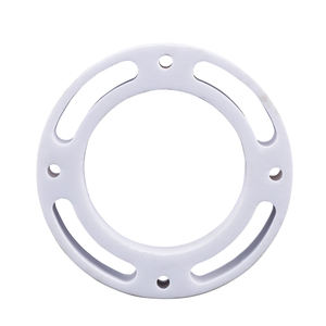
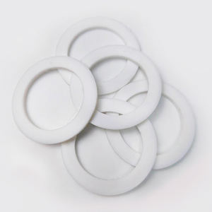
(アルミナセラミック基板)
Alumina ceramic substratums, mostly made up of light weight aluminum oxide (アル₂O₃), act as the backbone of modern electronic product packaging because of their phenomenal equilibrium of electrical insulation, 熱安定性, 機械的強度, and manufacturability.
The most thermodynamically steady phase of alumina at heats is corundum, or α-Al Two O TWO, which crystallizes in a hexagonal close-packed oxygen latticework with aluminum ions occupying two-thirds of the octahedral interstitial websites.
This thick atomic plan imparts high hardness (Mohs 9), superb wear resistance, and solid chemical inertness, making α-alumina appropriate for rough operating environments.
Commercial substratums usually contain 90– 99.8% アル₂ フォー, with minor additions of silica (サイオツー), マグネシア (MgO), or uncommon earth oxides used as sintering aids to advertise densification and control grain development during high-temperature handling.
Greater pureness qualities (例えば, 99.5% and over) display remarkable electrical resistivity and thermal conductivity, while lower pureness variations (90– 96%) offer affordable solutions for less demanding applications.
1.2 Microstructure and Defect Design for Electronic Reliability
The efficiency of alumina substrates in digital systems is seriously based on microstructural harmony and issue reduction.
A fine, equiaxed grain structure– 通常は~からの範囲です 1 に 10 マイクロメートル– makes certain mechanical stability and lowers the probability of crack breeding under thermal or mechanical anxiety.
気孔率, especially interconnected or surface-connected pores, must be minimized as it degrades both mechanical toughness and dielectric performance.
Advanced processing strategies such as tape spreading, 静水圧プレス, and regulated sintering in air or managed environments enable the production of substrates with near-theoretical thickness (> 99.5%) and surface area roughness below 0.5 μm, crucial for thin-film metallization and cable bonding.
さらに, impurity segregation at grain borders can result in leak currents or electrochemical migration under prejudice, requiring rigorous control over raw material purity and sintering problems to make certain long-lasting integrity in moist or high-voltage environments.
2. Production Processes and Substratum Construction Technologies
( アルミナセラミック基板)
2.1 Tape Spreading and Eco-friendly Body Processing
The manufacturing of alumina ceramic substrates begins with the prep work of an extremely dispersed slurry containing submicron Al ₂ O three powder, organic binders, 可塑剤, dispersants, および溶剤.
This slurry is processed by means of tape spreading– a continuous method where the suspension is topped a relocating carrier film utilizing a precision medical professional blade to achieve uniform thickness, 通常は次の間で 0.1 mm and 1.0 mm.
After solvent dissipation, the resulting “eco-friendly tape” is flexible and can be punched, drilled, or laser-cut to form through openings for upright interconnections.
Multiple layers may be laminated to produce multilayer substrates for intricate circuit assimilation, although the majority of commercial applications use single-layer configurations due to set you back and thermal development considerations.
The environment-friendly tapes are then meticulously debound to eliminate organic additives with regulated thermal disintegration before last sintering.
2.2 Sintering and Metallization for Circuit Combination
Sintering is performed in air at temperatures in between 1550 ℃と 1650 ℃, where solid-state diffusion drives pore elimination and grain coarsening to achieve full densification.
The direct shrinkage throughout sintering– typically 15– 20%– need to be precisely forecasted and made up for in the style of environment-friendly tapes to make certain dimensional precision of the final substratum.
Complying with sintering, metallization is put on create conductive traces, pads, and vias.
2 key techniques dominate: thick-film printing and thin-film deposition.
In thick-film innovation, pastes having steel powders (例えば, タングステン, モリブデン, or silver-palladium alloys) are screen-printed onto the substratum and co-fired in a reducing ambience to develop durable, high-adhesion conductors.
For high-density or high-frequency applications, thin-film procedures such as sputtering or dissipation are utilized to down payment bond layers (例えば, titanium or chromium) complied with by copper or gold, enabling sub-micron pattern by means of photolithography.
Vias are full of conductive pastes and fired to develop electric interconnections between layers in multilayer styles.
3. Functional Qualities and Efficiency Metrics in Electronic Equipment
3.1 Thermal and Electric Habits Under Functional Tension
Alumina substrates are valued for their beneficial combination of moderate thermal conductivity (20– 35 W/m · K for 96– 99.8% アル₂ オー スリー), which makes it possible for reliable warm dissipation from power tools, and high quantity resistivity (> 10 ¹⁴ Ω・センチメートル), ensuring marginal leak current.
Their dielectric constant (εᵣ ≈ 9– 10 で 1 MHz) is secure over a wide temperature and regularity variety, making them appropriate for high-frequency circuits up to numerous ghzs, although lower-κ materials like light weight aluminum nitride are chosen for mm-wave applications.
The coefficient of thermal development (CTE) of alumina (~ 6.8– 7.2 ppm/K) is fairly well-matched to that of silicon (~ 3 ppm/K) and certain packaging alloys, lowering thermo-mechanical tension during gadget operation and thermal cycling.
しかし, the CTE mismatch with silicon stays a problem in flip-chip and straight die-attach setups, typically calling for compliant interposers or underfill products to minimize fatigue failing.
3.2 Mechanical Effectiveness and Environmental Durability
機械的に, alumina substratums show high flexural strength (300– 400 MPa) and excellent dimensional stability under lots, allowing their usage in ruggedized electronics for aerospace, 自動車, and commercial control systems.
They are immune to vibration, shock, and creep at raised temperatures, maintaining structural stability as much as 1500 不活性雰囲気では°C.
In moist atmospheres, high-purity alumina reveals minimal wetness absorption and outstanding resistance to ion movement, making certain long-term integrity in outside and high-humidity applications.
Surface firmness likewise secures versus mechanical damages during handling and assembly, although treatment should be taken to prevent edge chipping due to fundamental brittleness.
4. Industrial Applications and Technological Influence Across Sectors
4.1 Power Electronics, RF Modules, and Automotive Equipments
Alumina ceramic substrates are ubiquitous in power electronic modules, consisting of insulated gate bipolar transistors (IGBT), MOSFET, and rectifiers, where they provide electric isolation while promoting heat transfer to warmth sinks.
In radio frequency (RF) and microwave circuits, they function as service provider systems for hybrid integrated circuits (HICs), surface area acoustic wave (SAW) filters, and antenna feed networks due to their secure dielectric homes and reduced loss tangent.
In the auto market, alumina substratums are utilized in engine control devices (ECUs), sensor plans, and electric lorry (EV) power converters, where they withstand heats, サーマルバイク, and direct exposure to destructive liquids.
Their dependability under severe problems makes them important for safety-critical systems such as anti-lock braking (ABDOMINAL MUSCLE) and progressed driver help systems (ADAS).
4.2 Medical Instruments, 航空宇宙, and Arising Micro-Electro-Mechanical Solutions
Beyond customer and industrial electronics, alumina substratums are utilized in implantable clinical devices such as pacemakers and neurostimulators, where hermetic sealing and biocompatibility are vital.
航空宇宙および防衛分野, they are made use of in avionics, radar systems, and satellite interaction modules as a result of their radiation resistance and stability in vacuum cleaner settings.
さらに, alumina is increasingly used as a structural and protecting system in micro-electro-mechanical systems (MEMS), consisting of pressure sensors, accelerometers, and microfluidic tools, where its chemical inertness and compatibility with thin-film handling are beneficial.
As digital systems remain to require greater power thickness, 小型化, and integrity under severe conditions, alumina ceramic substratums continue to be a keystone product, linking the space in between efficiency, expense, and manufacturability in innovative digital product packaging.
5. サプライヤー
アルミナテクノロジー株式会社, Ltdは研究開発に重点を置いています, 酸化アルミニウム粉末の製造・販売, 酸化アルミニウム製品, 酸化アルミニウムるつぼ, 等, 電子機器のサービスを提供する, セラミックス, 化学およびその他の産業. 創業以来、 2005, 同社は顧客に最高の製品とサービスを提供することに尽力してきました。. 高品質を求めるなら アルミナal2o3, お気軽にお問い合わせください. ([email protected])
タグ: アルミナセラミック基板, アルミナセラミックス, アルミナ
すべての記事と写真はインターネットからのものです. 著作権上の問題がある場合, 削除するには時間内にご連絡ください.
お問い合わせください
https://www.aluminumoxide.co.uk/products/nano-alumina-powder/
This nano-alumina powder is of exceptional quality, exceeding my expectations. Its purity is extremely high, and its particle size distribution is uniform and very fine, reaching the true nanometer level. It also exhibits excellent dispersion and virtually no agglomeration, greatly facilitating subsequent applications. I’m using it for ceramic toughening. The technical specifications provided by the supplier are detailed and reliable, highly consistent with actual test results.