


1. Awọn ipilẹ ohun elo ati Awọn didara ayaworan ti Awọn ohun elo Alumina
1.1 Crystallographic ati Ipilẹ Iṣọkan ti α-Alumina
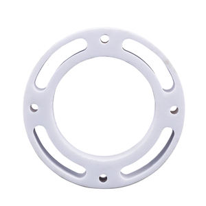
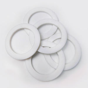
(Alumina seramiki Sobsitireti)
Alumina seramiki substratums, okeene ṣe soke ti ina àdánù aluminiomu oxide (Al ₂ O₃), ṣe bi egungun ẹhin ti iṣakojọpọ ọja eletiriki ode oni nitori iwọntunwọnsi iyalẹnu wọn ti idabobo itanna, gbona iduroṣinṣin, darí agbara, ati iṣelọpọ.
Ipele imuduro thermodynamic julọ julọ ti alumina ni awọn igbona jẹ corundum, tabi α-Al Meji O MEJI, eyi ti o crystallizes ni hexagonal isunmọ-aba ti atẹgun latticework pẹlu aluminiomu ions ti o gba meji-meta ti awọn aaye ayelujara interstitial octahedral.
Eto atomiki ti o nipọn yii funni ni lile lile (Mohs 9), to dara julọ yiya resistance, ati ki o ri to kemikali inertness, ṣiṣe α-alumina ti o yẹ fun awọn agbegbe iṣẹ inira.
Substratums ti iṣowo nigbagbogbo ni 90 ninu– 99.8% Al ₂ O KẸRIN, pẹlu awọn afikun kekere ti yanrin (SiO MEJI), magnẹsia (MgO), tabi awọn oxides aiye ti ko wọpọ ti a lo bi awọn iranlọwọ sintering lati polowo densification ati iṣakoso idagbasoke ọkà lakoko mimu iwọn otutu giga..
Greater funfun ànímọ (f.eks., 99.5% ati lori) han o lapẹẹrẹ itanna resistivity ati ki o gbona iba ina elekitiriki, lakoko awọn iyatọ mimọ kekere (90– 96%) pese awọn solusan ti ifarada fun awọn ohun elo ti o kere ju.
1.2 Microstructure ati Apẹrẹ Aṣiṣe fun Igbẹkẹle Itanna
Iṣiṣẹ ti awọn sobusitireti alumina ni awọn eto oni-nọmba jẹ pataki da lori isokan microstructural ati idinku ọrọ.
A itanran, equiaxed ọkà be– maa orisirisi lati 1 si 10 micrometers– mu ki awọn darí iduroṣinṣin ati kekere ti awọn iṣeeṣe ti kiraki ibisi labẹ gbona tabi darí ṣàníyàn.
Porosity, paapa interconnected tabi dada-so pores, gbọdọ wa ni o ti gbe sẹgbẹ bi o ti degrades mejeeji darí toughness ati dielectric išẹ.
To ti ni ilọsiwaju ilana ilana bi teepu itankale, isostatic titẹ, ati isunmọ ilana ni afẹfẹ tabi awọn agbegbe iṣakoso jẹ ki iṣelọpọ ti awọn sobusitireti pẹlu sisanra-ijinlẹ isunmọ (> 99.5%) ati dada agbegbe roughness ni isalẹ 0.5 µm, pataki fun tinrin-fiimu metallization ati USB imora.
Ni afikun, ipinya aimọ ni awọn aala ọkà le ja si awọn ṣiṣan ṣiṣan tabi iṣilọ elekitiroki labẹ ikorira, nilo iṣakoso to muna lori mimọ ohun elo aise ati awọn iṣoro sisọnu lati ṣe iduroṣinṣin pipẹ ni awọn agbegbe tutu tabi awọn agbegbe foliteji giga..
2. Awọn ilana iṣelọpọ ati Awọn imọ-ẹrọ Ikole Substratum
( Alumina seramiki Sobsitireti)
2.1 Teepu Itankale ati Eco-ore Ara Processing
Ṣiṣejade ti awọn sobusitireti seramiki alumina bẹrẹ pẹlu iṣẹ igbaradi ti slurry ti a tuka kaakiri pupọ ti o ni submicron Al ₂ O lulú mẹta., Organic binders, pilasitik, dispersants, ati olomi.
Yi slurry ti wa ni ilọsiwaju nipasẹ ọna ti ntan teepu– ọna lemọlemọfún nibiti idaduro naa ti dofun fiimu gbigbe gbigbe kan ni lilo abẹfẹlẹ ọjọgbọn iṣoogun ti konge lati ṣaṣeyọri sisanra aṣọ., ojo melo laarin 0.1 mm ati 1.0 mm.
Lẹhin ipadanu olomi, Abajade “irinajo-friendly teepu” jẹ rọ ati ki o le ti wa ni punched, ti gbẹ iho, tabi lesa-ge lati dagba nipasẹ šiši fun pipe interconnections.
Ọpọ fẹlẹfẹlẹ le wa ni laminated lati gbe awọn multilayer sobsitireti fun intricate Circuit assimilation, botilẹjẹpe pupọ julọ awọn ohun elo iṣowo lo awọn atunto Layer-ẹyọkan nitori lati ṣeto ọ pada ati awọn ero idagbasoke igbona.
Awọn teepu ore-ayika naa yoo yọkuro daradara lati yọkuro awọn afikun Organic pẹlu itusilẹ igbona ti a ṣe ilana ṣaaju isunmọ to kẹhin..
2.2 Sintering ati Metallization fun Circuit Apapo
Sintering ni a ṣe ni afẹfẹ ni awọn iwọn otutu laarin 1550 ° C ati 1650 ° C, ibi ti ri to-ipinle tan kaakiri iwakọ pore imukuro ati ọkà coarsening lati se aseyori ni kikun densification.
Awọn taara isunki jakejado sintering– deede 15– 20%– nilo lati ṣe asọtẹlẹ ni deede ati ṣe apẹrẹ fun ara ti awọn teepu ore-ayika lati ṣe deede iwọn iwọn kan ti substratum ikẹhin.
Ni ibamu pẹlu sintering, metallization ti wa ni fi lori ṣẹda conductive tọpasẹ, paadi, ati vias.
2 bọtini imuposi gaba lori: titẹjade fiimu ti o nipọn ati fifisilẹ fiimu tinrin.
Ni nipọn-fiimu ĭdàsĭlẹ, pastes nini irin powders (f.eks., tungsten, molybdenum, tabi fadaka-palladium alloys) ti wa ni titẹ-iboju sori sobusitireti ati ki o ṣajọpọ ni ambience idinku lati ṣe idagbasoke ti o tọ, ga-adhesion conductors.
Fun iwuwo giga tabi awọn ohun elo igbohunsafẹfẹ giga, awọn ilana fiimu tinrin gẹgẹbi sputtering tabi dissipation ti wa ni lilo si isalẹ awọn fẹlẹfẹlẹ mnu sisanwo (f.eks., titanium tabi chromium) complied pẹlu Ejò tabi wura, muu ilana iha-micron ṣiṣẹ nipasẹ ọna fọtolithography.
Vias ti kun fun awọn lẹẹ adaṣe ati ina lati ṣe agbekalẹ awọn asopọ ina mọnamọna laarin awọn fẹlẹfẹlẹ ni awọn aza multilayer.
3. Awọn agbara iṣẹ ṣiṣe ati Awọn Metiriki Iṣiṣẹ ni Awọn ohun elo Itanna
3.1 Gbona ati Ina Awọn isesi Labẹ Ẹdọfu Iṣẹ
Awọn sobusitireti alumina ni idiyele fun apapọ anfani wọn ti iṣiṣẹ igbona iwọntunwọnsi (20– 35 W/m · K fun 96– 99.8% Al ₂ O META), eyi ti o jẹ ki o ṣee ṣe fun igbẹkẹle gbigbona ti o gbẹkẹle lati awọn irinṣẹ agbara, ati ki o ga opoiye resistivity (> 10 ¹⁴ Ω · sẹntimita), aridaju iwonba jo lọwọlọwọ.
Wọn dielectric ibakan (εᵣ≈ 9– 10 ni 1 MHz) ni aabo lori kan jakejado otutu ati regularity orisirisi, ṣiṣe wọn yẹ fun awọn iyika igbohunsafẹfẹ-giga to awọn ghzs lọpọlọpọ, botilẹjẹpe awọn ohun elo kekere-κ bii iwuwo nitride aluminiomu iwuwo ni a yan fun awọn ohun elo igbi-mm.
Awọn iyeida ti gbona idagbasoke (CTE) ti aluminiomu (~ 6.8– 7.2 ppm/K) ti wa ni iṣẹtọ daradara-ti baamu si ti ohun alumọni (~ 3 ppm/K) ati awọn alloys apoti kan, sokale thermo-darí ẹdọfu nigba ẹrọ irinṣẹ ati ki o gbona gigun kẹkẹ.
Sibẹsibẹ, aiṣedeede CTE pẹlu ohun alumọni duro iṣoro kan ni chip-pip ati awọn iṣeto di-somọ taara, ojo melo pipe fun ifaramọ interposers tabi underfill awọn ọja lati gbe rirẹ aise.
3.2 Ṣiṣe ẹrọ ati Itọju Ayika
Mekaniki, alumina substratums ṣe afihan agbara rirọ giga (300– 400 MPa) ati iduroṣinṣin onisẹpo ti o dara julọ labẹ ọpọlọpọ, gbigba wọn lilo ni gaungaun Electronics fun Aerospace, ọkọ ayọkẹlẹ, ati awọn eto iṣakoso iṣowo.
Wọn jẹ ajesara si gbigbọn, mọnamọna, ati nrakò ni awọn iwọn otutu ti o ga, mimu iduroṣinṣin igbekale bi Elo bi 1500 ° C ni awọn ambiences inert.
Ni awọn agbegbe tutu, alumina mimọ-giga ṣe afihan gbigba ọrinrin pọọku ati atako to dayato si gbigbe ion, ṣiṣe awọn iṣotitọ igba pipẹ ni ita ati awọn ohun elo ọriniinitutu giga.
Imuduro dada bakanna ni aabo ni ilodisi awọn ibajẹ ẹrọ lakoko mimu ati apejọ, botilẹjẹpe o yẹ ki o gba itọju lati yago fun gige eti nitori brittleness ipilẹ.
4. Awọn ohun elo Ile-iṣẹ ati Ipa Imọ-ẹrọ Kọja Awọn apakan
4.1 Agbara Electronics, Awọn modulu RF, ati Automotive Equipments
Awọn sobusitireti seramiki Alumina wa ni ibi gbogbo ni awọn modulu itanna agbara, ti o ni awọn transistors ẹnu-ọna bipolar ti o ya sọtọ (Awọn IGBT), MOSFET, ati awọn atunṣe, nibiti wọn ti pese iyasọtọ ina mọnamọna lakoko igbega gbigbe ooru si awọn ifọwọ igbona.
Ni igbohunsafẹfẹ redio (RF) ati makirowefu iyika, wọn ṣiṣẹ bi awọn ọna ṣiṣe olupese iṣẹ fun awọn iyika iṣọpọ arabara (Awọn HIC), dada akositiki igbi (SAW) Ajọ, ati awọn nẹtiwọọki ifunni eriali nitori awọn ile dielectric ti o ni aabo ati tangent isonu ti o dinku.
Ni awọn auto oja, alumina substratums ti wa ni lilo ninu awọn ẹrọ iṣakoso engine (Awọn ECU), sensọ eto, ati akẹru itanna (EV) agbara converters, ibi ti nwọn koju awọn ooru, gbona gigun keke, ati ifihan taara si awọn olomi iparun.
Igbẹkẹle wọn labẹ awọn iṣoro to lagbara jẹ ki wọn ṣe pataki fun awọn eto aabo-pataki gẹgẹbi idena titiipa (INU INU) ati awọn ọna ṣiṣe iranlọwọ awakọ ilọsiwaju (ADAS).
4.2 Awọn ohun elo iṣoogun, Ofurufu, ati Dide Micro-Electro-Mechanical Solutions
Ni ikọja onibara ati ẹrọ itanna ile-iṣẹ, Awọn substratums alumina ti wa ni lilo ninu awọn ẹrọ ile-iwosan ti a fi gbin gẹgẹbi awọn olutọpa ati awọn neurostimulators, nibiti lilẹ hermetic ati biocompatibility jẹ pataki.
Ni Aerospace ati olugbeja, wọn ti wa ni lilo ninu awọn avionics, Reda awọn ọna šiše, ati awọn modulu ibaraenisepo satẹlaiti bi abajade ti itọsi itankalẹ wọn ati iduroṣinṣin ni awọn eto imukuro igbale.
Siwaju sii, alumina ti wa ni lilo siwaju sii bi igbekalẹ ati eto aabo ni awọn ọna ṣiṣe micro-electro-mechanical (MEMS), ti o ni awọn sensọ titẹ, accelerometers, ati awọn irinṣẹ microfluidic, nibiti ailagbara kemikali rẹ ati ibaramu pẹlu mimu fiimu tinrin jẹ anfani.
Bi awọn eto oni-nọmba ṣe wa lati nilo sisanra agbara nla, miniaturization, ati iyege labẹ àìdá awọn ipo, awọn substratums seramiki alumina tẹsiwaju lati jẹ ọja bọtini bọtini, sisopo aaye laarin ṣiṣe, inawo, ati iṣelọpọ ni iṣakojọpọ ọja oni-nọmba tuntun.
5. Olupese
Alumina Technology Co., Ltd., Ltd idojukọ lori iwadi ati idagbasoke, isejade ati tita ti aluminiomu oxide lulú, aluminiomu ohun elo afẹfẹ, aluminiomu ohun elo afẹfẹ crucible, ati be be lo., sìn awọn ẹrọ itanna, amọ, kemikali ati awọn ile-iṣẹ miiran. Niwon awọn oniwe-idasile ni 2005, Ile-iṣẹ naa ti ṣe adehun lati pese awọn alabara pẹlu awọn ọja ati iṣẹ ti o dara julọ. Ti o ba n wa didara ga aluminiomu al2o3, jọwọ lero free lati kan si wa. ([email protected])
Awọn afi: Alumina seramiki Sobsitireti, Awọn ohun elo alumọni, aluminiomu
Gbogbo awọn nkan ati awọn aworan wa lati Intanẹẹti. Ti o ba wa eyikeyi awọn ọran aṣẹ lori ara, jọwọ kan si wa ni akoko lati parẹ.
Beere wa
https://www.aluminumoxide.co.uk/products/nano-alumina-powder/
Yi nano-alumina lulú jẹ didara ti o yatọ, ju ireti mi lọ. Awọn oniwe-nw jẹ lalailopinpin giga, ati awọn oniwe-patiku iwọn pinpin jẹ aṣọ ati ki o gidigidi itanran, de ipele nanometer otitọ. O tun ṣe afihan pipinka ti o dara julọ ati pe ko si agglomeration, irọrun pupọ awọn ohun elo atẹle. Mo n lo fun seramiki toughing. Awọn alaye imọ-ẹrọ ti a pese nipasẹ olupese jẹ alaye ati igbẹkẹle, gíga ni ibamu pẹlu awọn abajade idanwo gangan.